Method for producing transparent conductive film

a technology of transparent conductive film and conductive film, which is applied in the direction of vacuum evaporation coating, instruments, coatings, etc., to achieve the effects of reducing specific resistance, reducing crystallization time, and reducing crystallization tim

Inactive Publication Date: 2012-05-10
NITTO DENKO CORP
View PDF3 Cites 21 Cited by
  • Summary
  • Abstract
  • Description
  • Claims
  • Application Information

AI Technical Summary

Benefits of technology

[0031]It is considered that the effect of the invention to reduce crystallization time is produced by the feature that in the transparent conductive film including an indium-based complex oxide transparent conductive layer, a transparent conductive layer susceptible to crystallization is placed at a position susceptible to crystallization so that crystal growth in an amorphous transparent conductive layer less susceptible to crystallization can be facilitated.
[0032]As mentioned above, as the content of a tetravalent metal element oxide in an indium oxide material for a transparent conductive layer increases, current carriers increase, so that specific resistance decreases. Therefore, it has been considered that a reduction in specific resistance and a reduction in the content of a tetravalent metal element content for the purpose of reducing crystallization time are a trade-off or difficult to achieve at the same time. According to the invention, however, a reduction in crystallization time and a reduction in specific resistance can be achieved at the same time. In the method for producing the transparent conductive film of the invention, indium oxide or an indium-based complex oxide having a low tetravalent metal element oxide content is deposited at the front surface side of the transparent conductive layer. It is therefore considered that since the front surface side transparent conductive layer contains no tetravalent metal element oxide or has a low tetravalent metal element oxide content, the rate of substitution of the tetravalent metal element is rather increased by the acceleration of crystallization, so that the specific resistance can be reduced.

Problems solved by technology

Unfortunately, a transparent conductive film produced with a film substrate has a problem in which the upper limit of the heating temperature for the crystallization of the transparent conductive layer is lower than that in the case where a glass substrate is used, and therefore, the specific resistance of the crystallized transparent conductive layer is higher in the transparent conductive film than in the product having the glass substrate.

Method used


Image

  • Method for producing transparent conductive film
  • Method for producing transparent conductive film
  • Method for producing transparent conductive film

Examples


example 1

[0088]A 30 nm thick undercoat layer of a thermosetting resin composed of a melamine resin, an alkyd resin, and an organosilane condensate (2:2:1 in weight ratio) was formed on one surface of a film substrate made of a 23 μm thick polyethylene terephthalate film (hereinafter referred to as PET film). The surface of the undercoat layer had an arithmetic average roughness Ra of 0.5 nm.

[0089]A 20 nm thick deposited layer of an indium-tin complex oxide was formed on the undercoat layer by a reactive sputtering method using a sintered material of 90% indium oxide and 10% tin monoxide in a 0.4 Pa atmosphere composed of 80% by volume of argon gas and 20% by volume of oxygen gas. The deposition process included evacuating the sputtering system until the water partial pressure at the time of deposition reached 8.0×10⁻⁵ Pa, then introducing argon gas and oxygen gas, and performing the deposition at a substrate temperature of 140° C. in an atmosphere with a water partial pressure of 8.0×10⁻⁵ Pa...

examples 2 to 7 and 9 to 13

[0092]Transparent conductive films were prepared as in Example 1, except that the content of tin oxide in the sintered indium oxide-tin oxide material and the thickness of each layer, which were used in forming the deposited layer (22) in the step (A1) and in forming the deposited layer (21) in the step (A2), were changed as shown in Table 1. Each transparent conductive layer was also crystallized as in Example 1. In Table 1, “tin oxide content” indicates the content of tin oxide in the indium oxide or indium-tin complex oxide material used as the sputtering target. A tin oxide content of “0%” indicates the case using indium oxide. The thickness of the deposited layer indicates the thickness before the crystallization. The content of tin oxide and the thickness of the deposited layer are considered to be unchanged even after the crystallization.

example 8

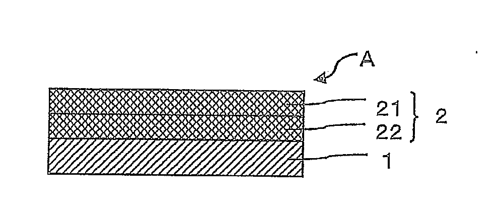
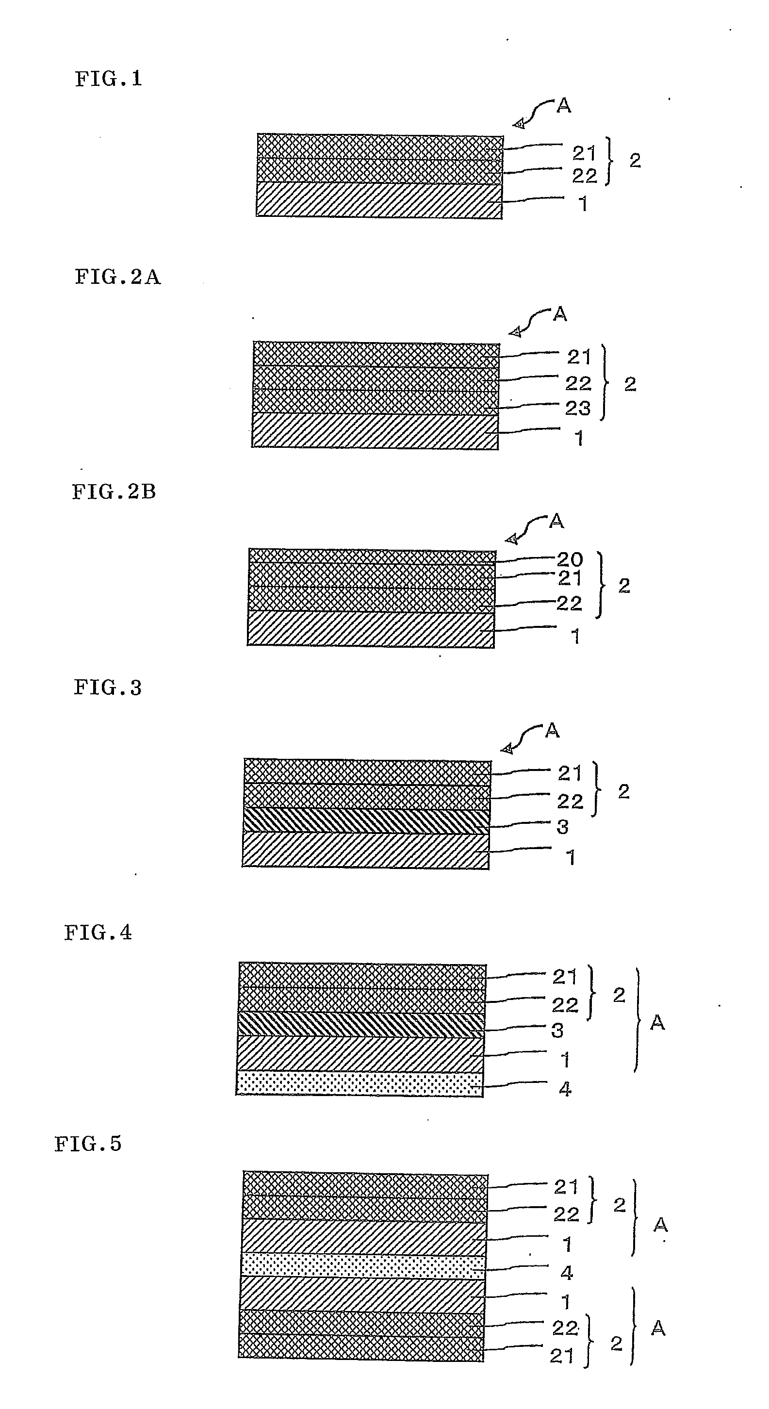
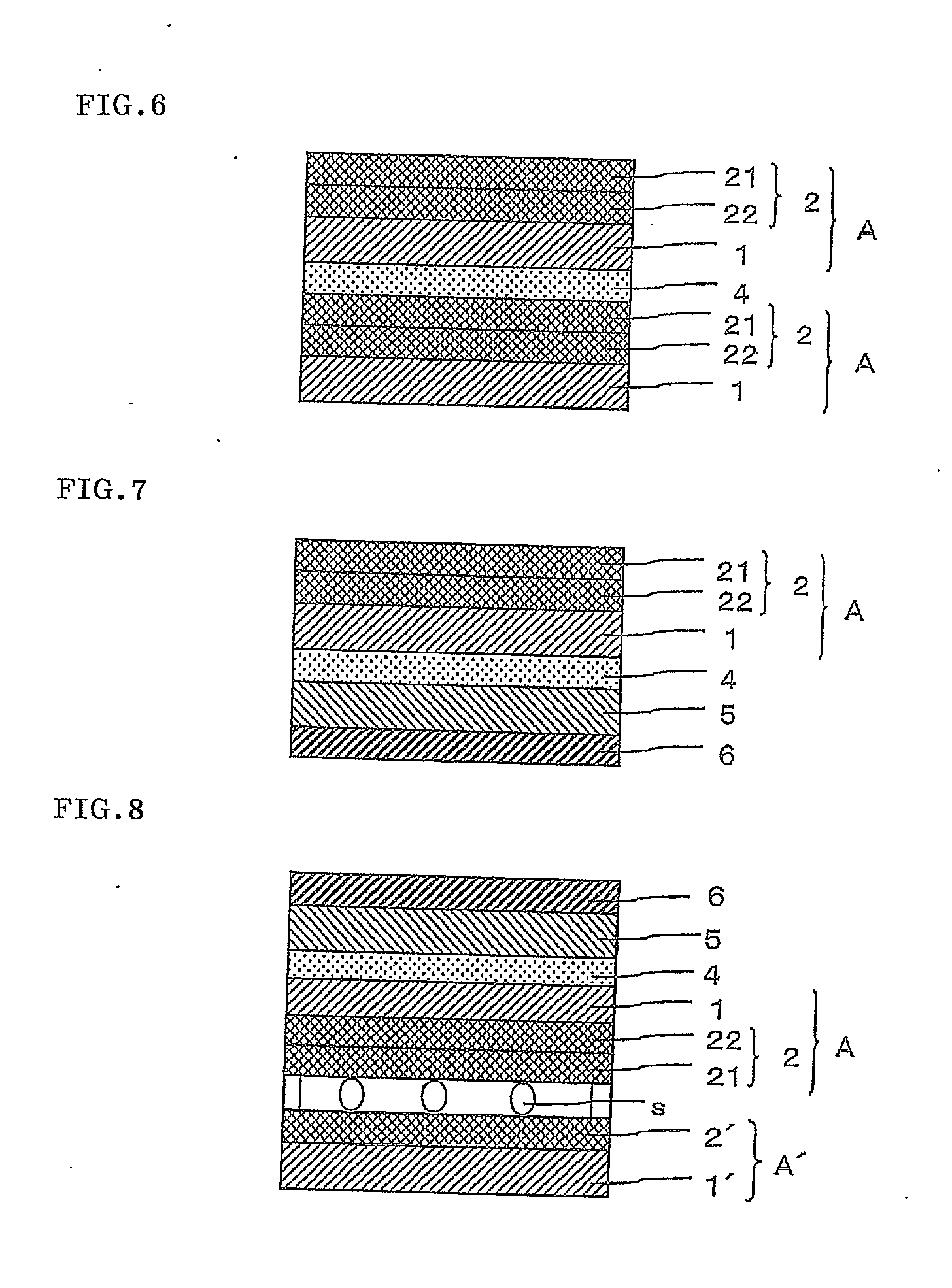
[0093]An undercoat layer was formed on one surface of a film substrate as in Example 1. A 3 nm thick deposited layer of an indium-tin complex oxide was formed on the undercoat layer by a reactive sputtering method using a sintered material of 97% indium oxide and 3% tin monoxide in a 0.4 Pa atmosphere composed of 80% by volume of argon gas and 20% by volume of oxygen gas. The deposition process included evacuating the sputtering system until the water partial pressure at the time of deposition reached 8.0×10⁻⁵ Pa, then introducing argon gas and oxygen gas, and performing the deposition at a substrate temperature of 140° C. in an atmosphere with a water partial pressure of 8.0×10⁻⁵ Pa. At this time, the water partial pressure was 0.05% of the partial pressure of the argon gas. The resulting deposited layer corresponds to the deposited layer (23) of FIG. 2A formed in another step.

[0094]A 19 nm thick deposited layer of an indium-tin complex oxide was further formed on the resulting dep...


PUM

PropertyMeasurementUnit
thicknessaaaaaaaaaa
thicknessaaaaaaaaaa
thicknessaaaaaaaaaa

Abstract

A method for producing a transparent conductive film including a transparent film substrate and a crystalline transparent conductive layer, including: a first depositing a first indium-based complex oxide having a first tetravalent metal element oxide on the transparent film substrate; and a second depositing indium oxide or a second indium-based complex oxide and lower than the tetravalent metal element oxide content of the indium-based complex oxide used in the first depositing by sputtering to form an amorphous transparent conductive layer, and crystallizing the amorphous transparent conductive layer. The method allows a reduction in crystallization time.

Description

BACKGROUND OF THE INVENTION[0001]1. Field of the Invention[0002]The invention relates to a method for producing a transparent conductive film having transparency in the visible light region and including a film substrate and a transparent conductive layer that is provided on the film substrate. The transparent conductive film obtained by the method of the invention is used for transparent electrodes in touch panels or displays such as liquid crystal displays and electroluminescence displays and also used for electromagnetic wave shielding or prevention of static buildup on transparent products. According to position detection method, touch panels may be classified into optical, ultrasonic, capacitance, and resistive touch panels. The transparent conductive film obtained by the method of the invention is suitable for use in capacitance touch panels, specifically, projection-type capacitance touch panels.[0003]2. Description of the Related Art[0004]Concerning a conventional transparen...

Claims


Application Information

Patent Timeline
Patent Type & Authority Applications(United States)
IPC IPC(8): C23C14/34
CPCC23C14/086C23C14/5806G06F2203/04103G06F3/045G06F3/044G06F3/0412
Inventor HAISHI, MOTOKINASHIKI, TOMOTAKENOGUCHI, TOMONORIASAHARA, YOSHIFUMI
Owner NITTO DENKO CORP
Why Eureka
Try Eureka