Apparatus for manufacturing a hierarchical structure

a hierarchical structure and apparatus technology, applied in the direction of mechanical control devices, process and machine control, instruments, etc., can solve the problems of inability to easily deform, the product using organic materials has a drawback in poor performance compared to silicon semiconductors or compound semiconductors, and the degree of integration of technology is limited, so as to improve productivity and improve productivity, the effect of deteriorating the data processing speed of organic semiconductors

Active Publication Date: 2012-05-17
KOREA INST OF MASCH & MATERIALS
View PDF3 Cites 27 Cited by
  • Summary
  • Abstract
  • Description
  • Claims
  • Application Information

AI Technical Summary

Benefits of technology

[0070]The effects of the prevent invention are as follow.
[0071]First, high performance elements and structures developed based on conventional semiconductor technology and nano technology can be formed on a flexible substrate. Through this, performance improvement may be 10 to 100 times of a conventional flexible product using an organic material. For example, the charge transfer speed of an organic semiconductor that has been tried to be applied to a flexible product is lower than one to one hundredth compared to that of the silicon semiconductor, and therefore the data processing speed of the organic semiconductor is deteriorated more than 100 times compared to the silicon semiconductor.
[0072]Second, productivity can be remarkably improved. The merit of the printed electronics using a conventional roll-to-roll printing is improvement of productivity, and the present invention also remarkably improve productivity through a manufacturing system using a roller and a belt.
[0073]Third, a product can be manufacture by mass-assembling large-scaled various elements and structures. A conventional roll-to-roll printing technology has limits in manufacturing of a structure that is smaller than 10 to 20 um, but the manufacturing system according to the present invention can overcome the size limit and various-scaled elements and structures can be hierarchically assembled to manufacture a product.

Problems solved by technology

However, recently, a semiconductor-associated processing technology has been extended to a nano area so that the technology has a limit in improvement of the degree of integration.
Meanwhile, a conventional flexible product manufacturing technology focused on using various polymer-based organic materials, but the product using the organic material has a drawback in poor performance compared to a silicon semiconductor or a compound semiconductor.
On the contrary, the silicon semiconductor or the compound semiconductor has excellent performance but also has strong brittleness so that it cannot be easily deformed and application to a flexible product is not ease.

Method used


Image

  • Apparatus for manufacturing a hierarchical structure
  • Apparatus for manufacturing a hierarchical structure
  • Apparatus for manufacturing a hierarchical structure

Examples


first exemplary embodiment

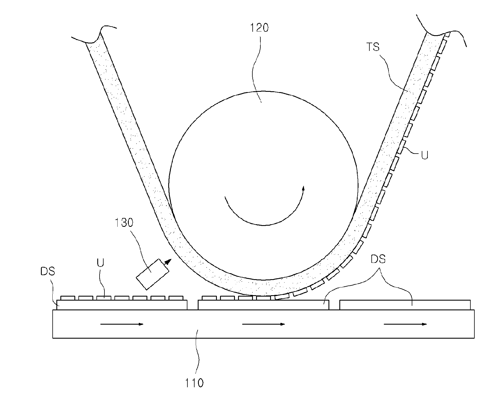
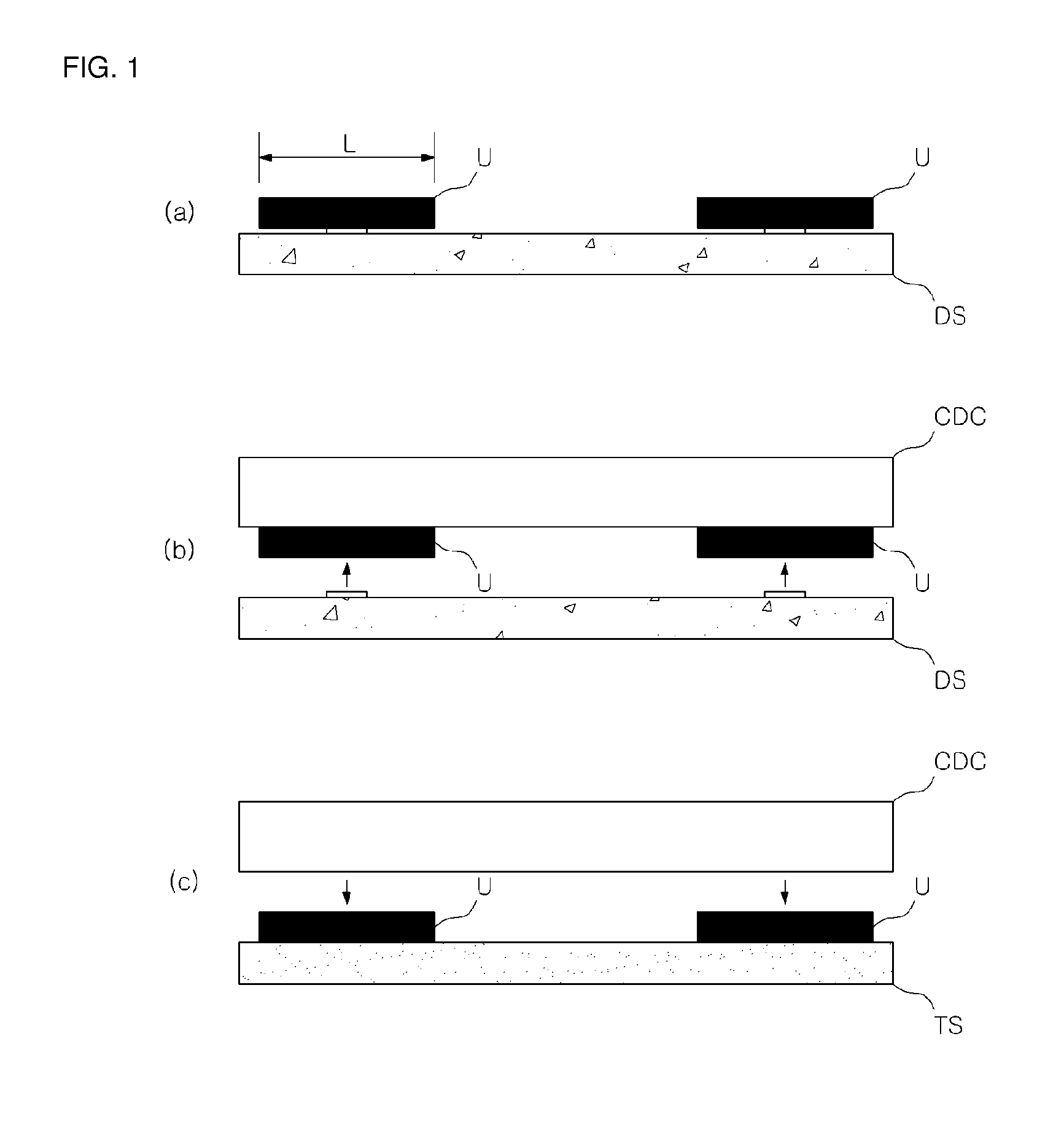
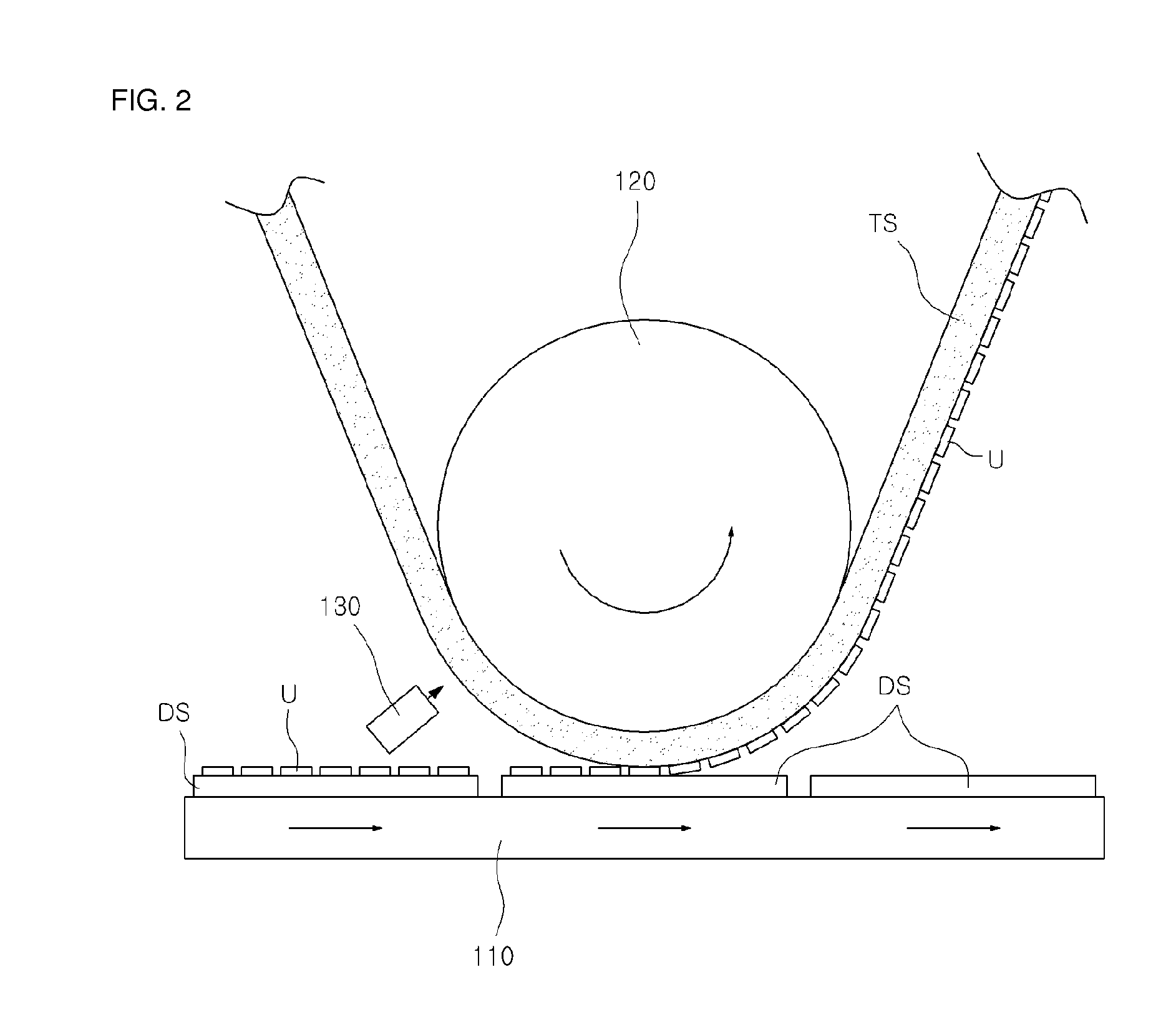
[0090]An apparatus for manufacturing a hierarchical structure according to the first exemplary embodiment releases a micro unit U provided on a dummy substrate DS made of a hard material to layer the same on a target substrate TS made of a flexible material, and includes a transfer stage 110 and a main roller 120, as shown in FIG. 2.

[0091]The transfer stage 110 is provided for flat-transferring of the dummy substrate DS by supporting the same, and for example, may be formed of a system such as a conveyor.

[0092]A micro unit U is provided on an upper surface of the dummy substrate DS flat-transferred by the transfer stage 110, and the micro unit U formed through a high-temperature process such as doping, oxidation, high-temperature thin film deposition, and RTP may include a high performance silicon semiconductor, a compound semiconductor, a micro structure, and a nano structure. The micro unit U may include an interconnection line for electrical connection and a nano structure for pe...

second exemplary embodiment

[0107]An apparatus for manufacturing a hierarchical structure according to the second exemplary embodiment includes a transfer stage 210, a sub roller 220, and a main roller 230 as shown in FIG. 3, and the transfer stage 210 is the same as the transfer stage 110 of the first exemplary embodiment and therefore no further description will be provided. A dummy substrate DS, a target substrate TS, and a micro unit U of the second exemplary embodiment are also the same as those of the first exemplary embodiment, and therefore no further description will be provided.

[0108]As the sub roller 220 contacts and the dummy substrate DS and thus rotates with pressure, the micro unit U of the dummy substrate DS is attached to an external circumference of the micro unit U. As shown in (a) of FIG. 4, the sub roller 220 is formed of a flexible polymer layer 222a and a core 224a. The polymer layer 222a as a predetermined thickness and the core 224a is formed strongly.

[0109]The polymer layer 222a is fo...

third exemplary embodiment

[0132]As shown in FIG. 5, an apparatus for manufacturing a hierarchical structure according to a third exemplary embodiment includes a transfer stage 310, a first sub roller 320, a second sub roller 330, a ring belt 340, a first tension roller 350, and a second tension roller 360, and the transfer stage 310 is the same as the transfer stage 110 of the first exemplary embodiment and therefore no further description will be described. A dummy substrate DS, a target substrate TS, and a micro unit U of the third exemplary embodiment are the same as those of the first exemplary embodiment, and therefore no further description will be provided.

[0133]The first sub roller 320 and the second sub roller 330 are provided to circulate the ring belt 340. The first sub roller 320 is disposed close to a micro unit U provided on an upper surface of a flat-transferred dummy substrate DS and the second sub roller 330 is disposed at a predetermined distance from the first sub roller 320.

[0134]The ring...


PUM

PropertyMeasurementUnit
sizeaaaaaaaaaa
temperatureaaaaaaaaaa
flexibleaaaaaaaaaa

Abstract

The present invention relates to an apparatus for massive manufacturing a hierarchical structure that can hierarchically form high performance micro units one a flexible substrate. For this purpose, an apparatus for manufacturing a hierarchical structure according to the present invention is provided to layer micro units provided on a dummy substrate that is made of a hard material on a target substrate that is made of a flexible material by releasing the micro units from the dummy substrate. The apparatus includes: a transfer stage flat-transferring the dummy substrate by supporting the same and a main roller rolling the target substrate by winding the same as the transfer stage proceeds and layering the micro unit of the dummy substrate on the target substrate.

Description

TECHNICAL FIELD[0001]The present invention relates to an apparatus for manufacturing a hierarchical structure. More particularly, the present invention relates to an apparatus for manufacturing a hierarchical structure. That is, a mass production manufacturing apparatus that can hierarchically form high performance micro units on a flexible substrate.BACKGROUND ART[0002]A technology related to a silicon semiconductor has been rapidly developed, and not only the silicon semiconductor but also various compound semiconductors can process mass data with high speed so that they offer great assistance to the human life in an optical element, optical communication, and wireless communication, leading IT revolution.[0003]The semiconductor-associated technology has been focused on high performance, large capacity, and ultrahigh speed through improvement of the degree of integration of the semiconductor. However, recently, a semiconductor-associated processing technology has been extended to ...

Claims


Application Information

Patent Timeline
Patent Type & Authority Applications(United States)
IPC IPC(8): B32B41/00B29C65/14H01L21/677B29C48/22
CPCH01L21/6836Y10T156/1705H01L24/95H01L25/0652H01L2221/68359H01L2221/68368H01L2224/7565H01L2224/83192H01L2224/838H01L2924/01013H01L2924/01047H01L2924/01057H01L2924/01082H01L2924/01005H01L2924/01006H01L2924/01019H01L2924/01033H01L2224/95145H01L2224/27312H01L2924/1461H01L24/83H01L2924/00Y10T156/1195Y10T156/1744B29C48/22H01L24/80B29C2043/463
Inventor KIM, JAE-HYUNLEE, HAK-JOOHYUN, SEUNG-MINHAN, SEUNG-WOOCHOI, BYUNG-IK
Owner KOREA INST OF MASCH & MATERIALS
Why Eureka
Try Eureka