Insulation circuit board, and power semiconductor device or inverter module using the same

a technology of insulation circuit board and power semiconductor device, which is applied in the direction of overvoltage circuit protection, electrical apparatus construction details, printed circuit aspects, etc., can solve the problems of short time-consuming and difficult to meet the requirements of use, and achieve high insulation reliability, low cost, and improved partial discharge resistance characteristics

Active Publication Date: 2012-05-24
HITACHI LTD
View PDF1 Cites 21 Cited by
  • Summary
  • Abstract
  • Description
  • Claims
  • Application Information

AI Technical Summary

Benefits of technology

[0020]According to the invention, while using the conventional insulation circuit board construction and wiring pattern forming method, the electric field concentration at the end sections of the wiring pattern to which a high voltage is applied is reduced and partial-discharge-resistant characteristics are improved. Therefore, even in high-density mounted wirings in which a distance between the wiring patterns is small, the insulation circuit board having the high insulation reliability can be realized by low costs. Providing of the power semiconductor device or inverter module using the insulation circuit board and having the high insulation reliability can be realized.
[0021]Other objects, features, and advantages of the present invention will be apparent from the following description of the embodiments of the invention with reference to the accompanying drawings.

Problems solved by technology

However, since a high power switching element such as an insulated-gate bipolar transistor (IGBT) or the like is used as a power semiconductor device for electric power conversion or an inverter module in recent years, there is a problem of an excessive heat generation.
However, if a high voltage associated with the realization of the recent high power is always applied to such an insulation circuit board, such a problem that a dielectric breakdown occurs for a short time can occur.
There is consequently such a problem that an electric field is concentrated on the end sections of the wiring pattern 3 and the partial discharging 4 occurs easily at this portion as a starting point.

Method used


Image

  • Insulation circuit board, and power semiconductor device or inverter module using the same
  • Insulation circuit board, and power semiconductor device or inverter module using the same
  • Insulation circuit board, and power semiconductor device or inverter module using the same

Examples


first embodiment

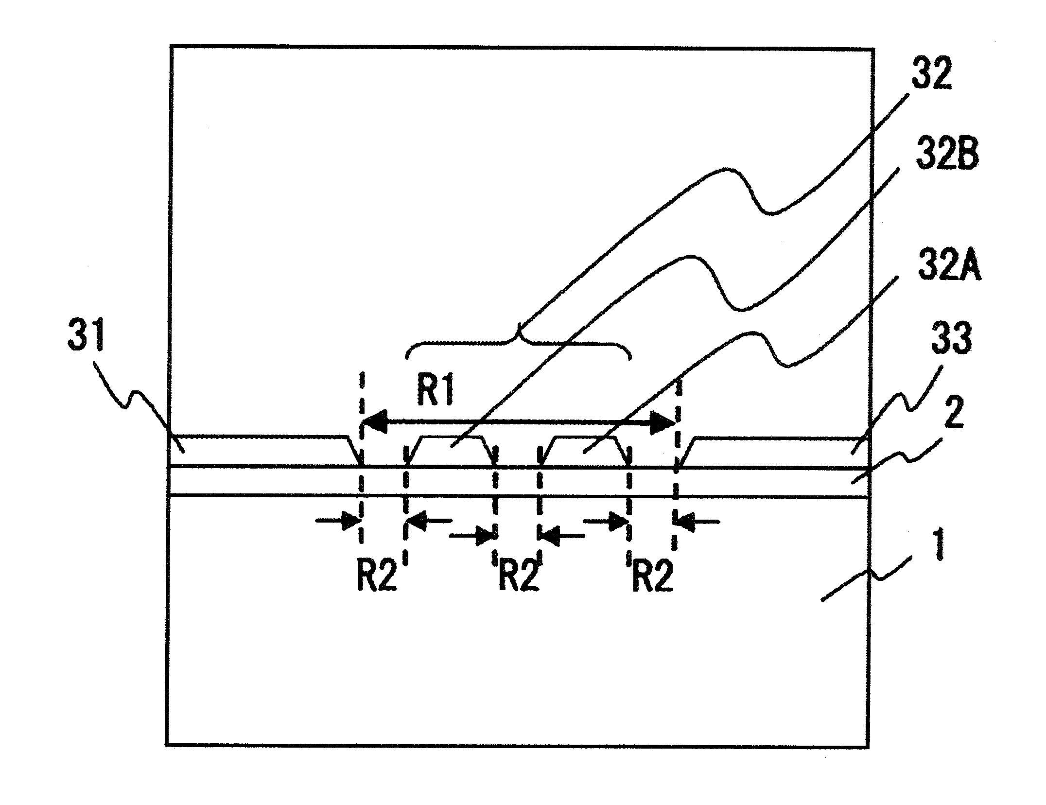
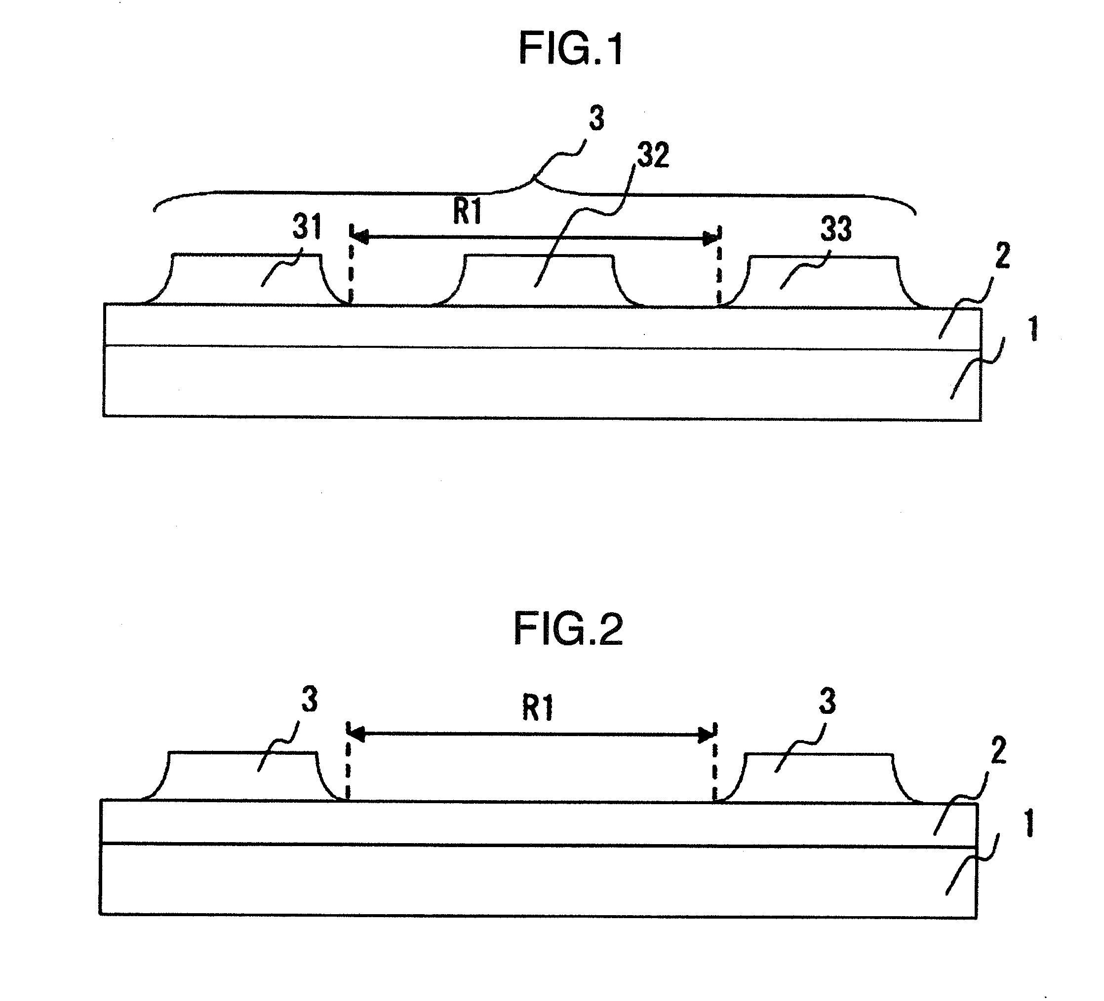
[0039]Each of FIGS. 1 and 6 is a cross sectional view of an insulation circuit board according to an embodiment of the invention. The embodiment illustrated in FIG. 6 has such a construction that in FIG. 2 showing a conventional embodiment, between adjacent wiring patterns 31 and 33 which are away from each other by the distance R1 between the wiring patterns, a new wiring pattern 32 is arranged at a position of a distance R2 between the wiring patterns corresponding to an equal distance from each of the wiring patterns 31 and 33. Other constructions are similar to those shown in FIG. 2 unless otherwise specified in particular.

[0040]The embodiment of FIG. 6 differs largely from the conventional embodiment with respect to a point that the wiring pattern 32 arranged between the adjacent wiring patterns 31 and 33 in FIG. 2 is voltage-divided by two resistors 8 and has an intermediate electric potential of an electric potential difference between the wiring patterns 31 and 33. For examp...

second embodiment

[0050]FIG. 8 shows an embodiment in the case where the invention is applied to a power semiconductor device or inverter module having an inverter circuit board of a motor control system.

[0051]In an outline of the inverter circuit of the motor control system, generally, as shown in a circuit diagram of FIG. 9, an inverter of three-phase outputs using six switching elements 9 is used. According to the inverter for the motor control, a DC current from a converter is input through a smoothing capacitor and is converted into a 3-phase alternating current by the switching element 9, thereby rotating the motor. A wiring construction shown in FIG. 8 here is obtained by presuming an inverter for a high output and six IGBT switching elements 9A to 9F and six free wheeling diodes 10A to 10F are mounted.

[0052]Among the wiring patterns 3 shown in FIG. 8 here, the wiring patterns which provide the highest potential difference are the wiring patterns between the input and the ground and an output ...

third embodiment

(Electric Field Simulation)

[0054]In order to verify an effect of the invention hereinbelow, analysis models are formed for the embodiments of the invention and comparative examples and local electric fields at the end sections of the high-potential wiring pattern 31 are derived by simulation.

[0055]FIG. 10 is a cross sectional model view for analyzing the insulation circuit board according to the embodiment of the invention.

[0056]The epoxy resin (dielectric constant: 4) insulation layer 2 having a thickness of 2.0 mmt is formed on the metal base substrate 1 having a thickness of 2.0 mmt and an electrolytic copper foil having a thickness of 0.1 mmt is further adhered onto the insulation layer 2. After that, the wiring patterns 31 and 33 formed by the chemical etching and the wiring pattern 32 according to the invention are formed onto the copper foil. An inclination angle of the side surface of each of the wiring patterns 31, 32, and 33 is equal to 60°. The wiring patterns 31 and 33 a...


PUM

PropertyMeasurementUnit
electric potentialaaaaaaaaaa

Abstract

The invention relates to a high-voltage insulation circuit board which is used in an electric power apparatus such as an electric power converter or the like such as power semiconductor device, inverter module, or the like and provides an insulation circuit board in which electric field concentration at the end sections of a wiring pattern is reduced, partial discharging is suppressed, and a reliability is high. According to the invention, there is provided an insulation circuit board having: a metal base substrate; and wiring patterns which are formed onto at least one of the surfaces of the metal base substrate through an insulation layer, characterized in that between two adjacent wiring patterns in which an electric potential difference exists among the wiring patterns, at least one or more wiring patterns or conductors which are in contact with the insulation layer and have an electric potential in a range of the electric potential difference between the adjacent wiring patterns are arranged. According to the invention, the electric field concentration at the end sections of the wiring pattern to which a high voltage is applied is reduced and partial-discharge-resistant characteristics are improved.

Description

INCORPORATION BY REFERENCE[0001]The present application claims priority from Japanese Patent Application JP2009-225903 filed on Sep. 30, 2009, the content of which is hereby incorporated by reference into this application.TECHNICAL FIELD[0002]The invention relates to a high-voltage insulation circuit board which is used in an electric power apparatus such as an electric power converter or the like such as power semiconductor device, inverter module, or the like and to a power semiconductor device or inverter module using such an insulation circuit board.BACKGROUND ART[0003]Hitherto, as an insulation circuit board for an electronic apparatus which is subjected to a severe temperature environment such as a vehicle-mounting environment or the like, a ceramic board having excellent heat radiation performance and heat resistance is a main stream. However, in association with a demand for low costs of the electronic apparatus, a shift to a resin board in which a high radiation insulation ...

Claims


Application Information

Patent Timeline
Patent Type & Authority Applications(United States)
IPC IPC(8): H05K7/04H05K1/05
CPCH01L23/142H01L23/49844H01L2924/0002H01L23/62H01L23/647H01L25/072H01L25/18H01L2924/09701H01L2924/12044H05K1/0256H05K1/0262H05K1/056H05K2201/0209H05K2201/0761H05K2201/09781H05K2201/10022H01L2924/00H05K1/0204H05K1/0257H05K1/053H05K2201/0154H05K2201/0162H02M7/003
Inventor MATSUMOTO, HIRONORIKUSUKAWA, JUMPEI
Owner HITACHI LTD
Why Eureka
Try Eureka