Dry etching method

a technology of dry etching and etching plate, which is applied in the testing/measurement of individual semiconductor devices, semiconductor/solid-state devices, instruments, etc., can solve the problems of adversely affecting the functions of mems devices, unable to obtain desired light reflection at the opening ha, etc., and suppresses the generation of notch. , the effect of positive charging of the exposed par

Active Publication Date: 2012-05-24
ULVAC INC
View PDF1 Cites 8 Cited by
  • Summary
  • Abstract
  • Description
  • Claims
  • Application Information

AI Technical Summary

Benefits of technology

[0012]Accordingly, it is an object of the present invention to provide a dry etching method capable of etching a silicon layer while suppressing undesired erosion of the silicon layer, that is, the generation of a notch, at a boundary of the silicon layer and an etching stopper layer.
[0016]In this method, the recess that extends through the silicon layer can be properly formed, while suppressing the generation of a notch in a preferable manner in accordance with various conditions, such as the thickness of the silicon layer of the substrate, the size of the opening of the recess, and the etching process.
[0022]As described above, when the etching stopper layer is exposed from part of the bottom surface of the recess, some of the etchant directed toward the bottom surface of the recess hits the etching stopper layer instead of the silicon layer. This decrease the amount of the etching produced generated by the reaction of the silicon layer and the etchant.
[0023]In the above method, the exposure of the etching stopper layer from part of the bottom surface of the recess is detected in the first step from a decrease in the generation amount of the etching product. Thus, the exposure of the etching stopper layer is detected in a preferable manner. This suppresses positive charging of the exposed part of the etching stopper layer caused by a delay in the shifting of the first step to the second step and ultimately suppresses the generation of the notch in a preferable manner.
[0026]In the above method, the exposure of the etching stopper layer from part of the bottom surface of the recess is detected in the first step from an increase in the generation amount of the etching product. Thus, the exposure of the etching stopper layer is detected in a preferable manner. This suppresses positive charging of the exposed part of the etching stopper layer caused by a delay in the shifting of the first step to the second step and ultimately suppresses the generation of the notch in a preferable manner.
[0028]In the above method, the sulfur hexafluoride gas is used as the raw material for fluorine radicals. The oxygen gas generates non-volatile oxide silicon fluoride in cooperation with the sulfur hexafluoride gas. The hydrogen bromide gas is used as the raw material for bromine ions that etch the silicon layer and generates oxide silicon bromide in cooperation with the oxygen gas. Thus, halide oxide silicon, such as oxide silicon fluoride and oxide silicon bromide, protects the side surface of the recess (silicon layer). Further, the etching of the bottom surface of the recess is enhanced by fluorine radicals and bromine ions. Thus the anisotropic etching is realized in a preferable manner.

Problems solved by technology

For instance, when the through hole H is used as an optical path for guiding light in the completed MEMS device, the desired light reflection at the opening Ha may not be obtained.
This may adversely affect the functions of the MEMS device.
Such problem occurs not only when etching a silicon layer used in a MEMS device but also when etching a silicon layer having a thickness of tens of micrometers to hundreds of micrometers and stacked on an etching stopper layer, which is formed by a dielectric, through the dry etching method shown in FIG. 4.

Method used


Image

  • Dry etching method
  • Dry etching method
  • Dry etching method

Examples


Embodiment Construction

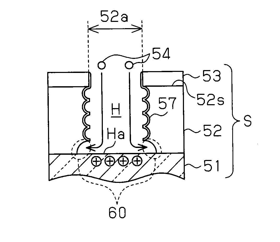
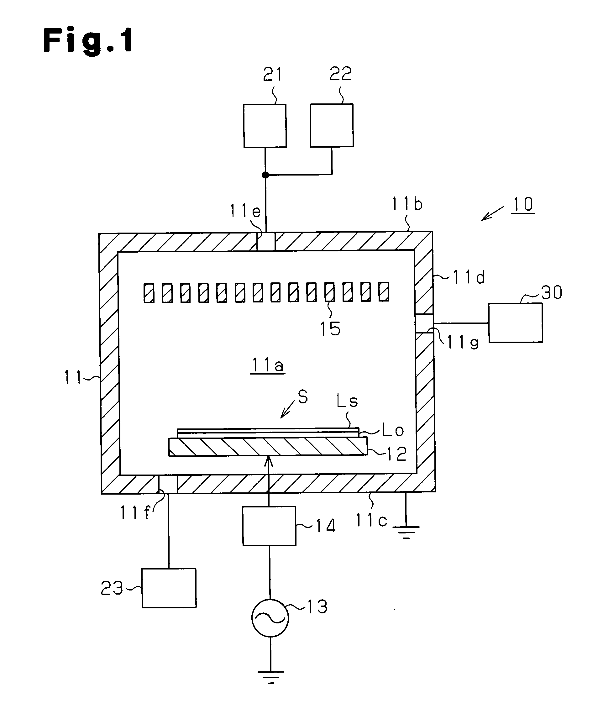
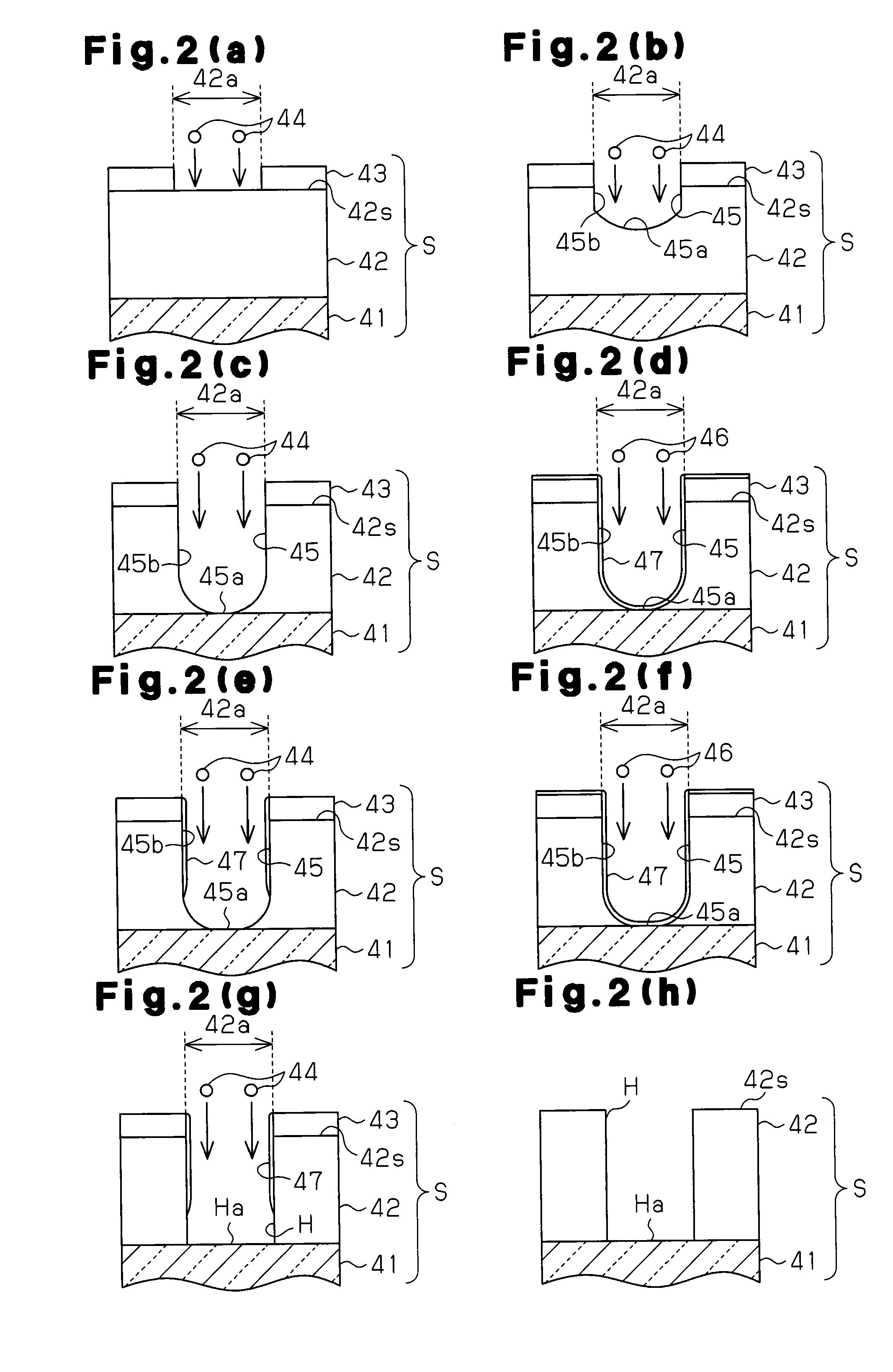
[0034]A dry etching method according to one embodiment of the present invention will now be described with reference to FIGS. 1 to 3. In this embodiment, a method for performing plasma etching on a silicon layer will be described.

[0035]FIG. 1 schematically shows the structure of a plasma etching device that performs etching using the plasma etching method of the present embodiment. As shown in FIG. 1, a substrate stage 12, on which a substrate S that is subject to processing is placed, is arranged in a plasma generation region 11a formed in a vacuum container 11 of the plasma etching device 10. The substrate S is a substrate for an MEMS device, for example, and includes a silicon oxide layer Lo, which serves as an etching stopper layer, and a silicon layer Ls, which is stacked on the silicon oxide layer Lo. The substrate S is arranged on the substrate stage 12 with the silicon oxide layer Lo being located at the lower side.

[0036]A high frequency power supply 13 is connected to the s...


PUM


Abstract

A dry etching method includes a first step and a second step. The first step includes generating a first plasma from a gas mixture, which includes an oxidation gas and a fluorine containing gas, and performing anisotropic etching with the first plasma on a silicon layer to form a recess in the silicon layer. The second step includes alternately repeating an organic film forming process whereby an organic film is deposited on the inner surface of the recess with a second plasma, and an etching process whereby the recess covered with the organic film is anisotropically etched with the first plasma. When an etching stopper layer is exposed from a part of the bottom surface of the recess formed in the first step, the first step is switched to the second step.

Description

RELATED APPLICATIONS[0001]The present application is a National Phase entry of PCT Application No. PCT / JP2011 / 051280, filed Jan. 25, 2011, which claims priority from Japanese Patent Application Number 2010-014792, filed Jan. 26, 2010, the disclosures of which are hereby incorporated by reference herein in their entirety.TECHNICAL FIELD[0002]The present invention relates to a dry etching method, and more particularly, to an anisotropic etching method for etching a silicon layer.BACKGROUND ART[0003]In the prior art, when, for example, manufacturing a so-called MEMS device including miniaturized mechanical components and electronic components, dry etching is employed to etch silicon layers used in the MEMS device. Patent document 1 describes the employment of reactive dry etching to form a pattern of recesses, through holes, and the like in a silicon layer of the MEMS device. A dry etching method of the prior art will now be described with reference to FIG. 4 based on patent document 1...

Claims


Application Information

Patent Timeline
Patent Type & Authority Applications(United States)
IPC IPC(8): H01L21/3065H01L21/66
CPCB81C1/00087H01L21/30655H01L21/3065B81C2201/0112
Inventor YOSHII, MANABUWATANABE, KAZUHIRO
Owner ULVAC INC
Why Eureka
Try Eureka