
Apparatus and method for detecting one or more analytes

a technology of apparatus and analytes, applied in the direction of instruments, superimposed coating processes, material impedance, etc., can solve the problem that their sensitivity still leaves scope for improvement, and achieve the effect of reliably detecting even lower concentrations of analytes and high sensitivity

Inactive Publication Date: 2012-05-31
MAX PLANCK GESELLSCHAFT ZUR FOERDERUNG DER WISSENSCHAFTEN EV
View PDF5 Cites 47 Cited by
  • Summary
  • Abstract
  • Description
  • Claims
  • Application Information

AI Technical Summary

Benefits of technology

[0007]The problem with all existing detectors is that their sensitivity still leaves scope for improvement. Thus, the present invention aims at achieving sensitivities in the sub-femtomolar range as low as 100 attomol (i.e. 10-16M) or possibly better. Furthermore, it is an object of the present invention to provide apparatus of the initially named kind which, despite being highly sensitive, can be manufactured economically and which represents a sound realization of the laboratory-on-a-chip concept.
[0010]Through the provision of the passivating layer it can be ensured that the functionalization of the elongate nanostructures does not lead to functionalization of the electrodes, which has been found to represent a major source of reduction of the detection sensitivity of the apparatus. The passivation layer also eliminates background electrical current which is caused by solution electrolytes present between electrodes. By the provision of a well in the substrate or in an insulating layer a liquid droplet containing the compound(s) used for functionalizing the elongate nanostructures can be brought into contact with the nanostructure(s), and this makes it very easy for the user or for an intermediary, such as a company selling chips, to prepare substrates (chips) for detecting specific analytes or groups of analytes. Furthermore, the well also enables the analyte(s) being investigated to be applied to the chips in a droplet of liquid so that any and all analytes present in the droplet can readily enter into contact with any or all the elongate nanostructures accessible through the respective well.
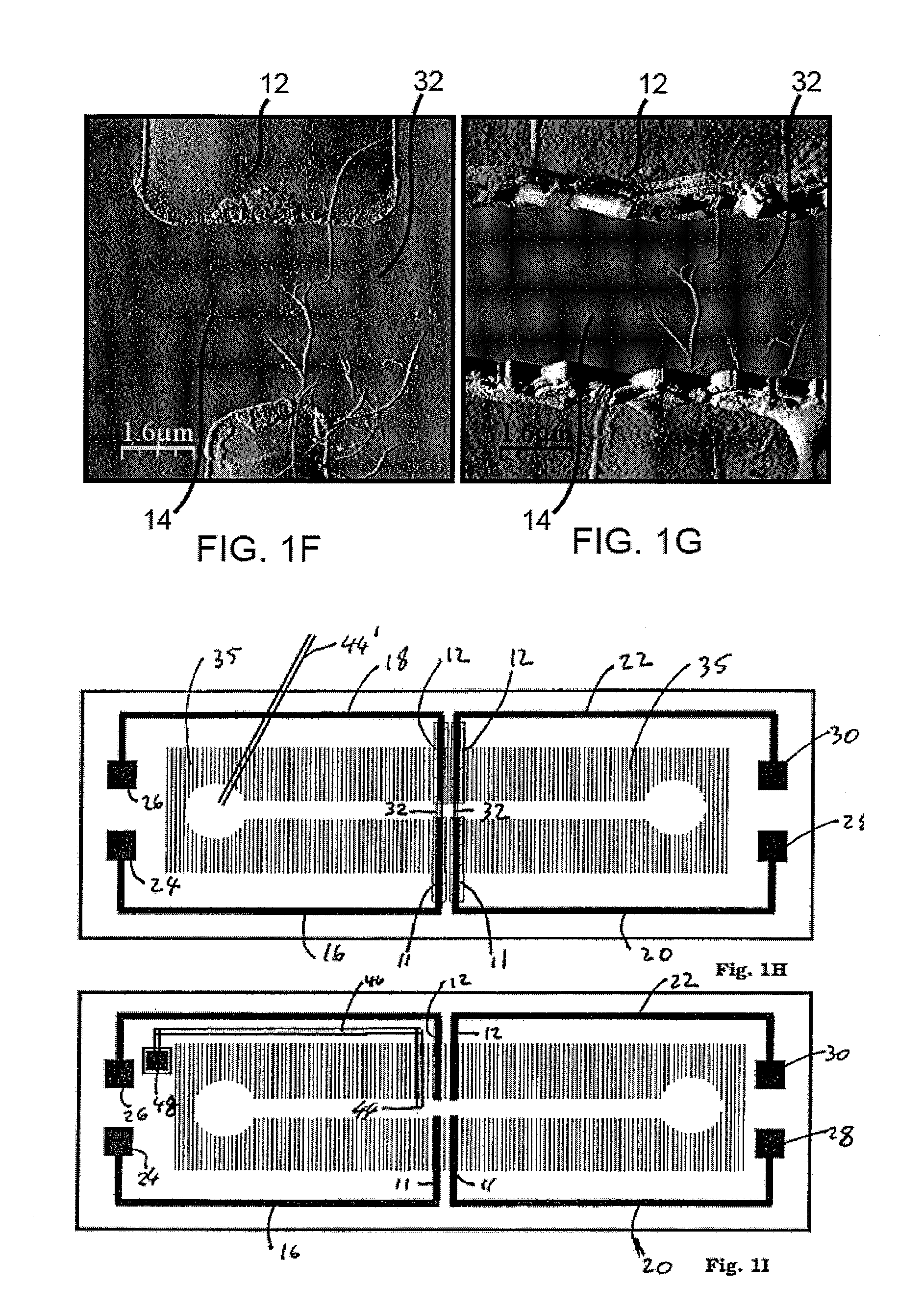
[0012]Furthermore, by providing a reference electrode on the substrate or dipping it into a liquid volume contained in the well, the reference electrode can act both as a gate and as a reference which greatly facilitates the calibration and readout from the individual FETs. This is especially useful when a plurality of elongate nanostructures are present extending away from one electrode and are all exposed to the same reactant within the well irrespective of whether they are all functionalized to detect the same analyte or are functionalized to detect different analytes.
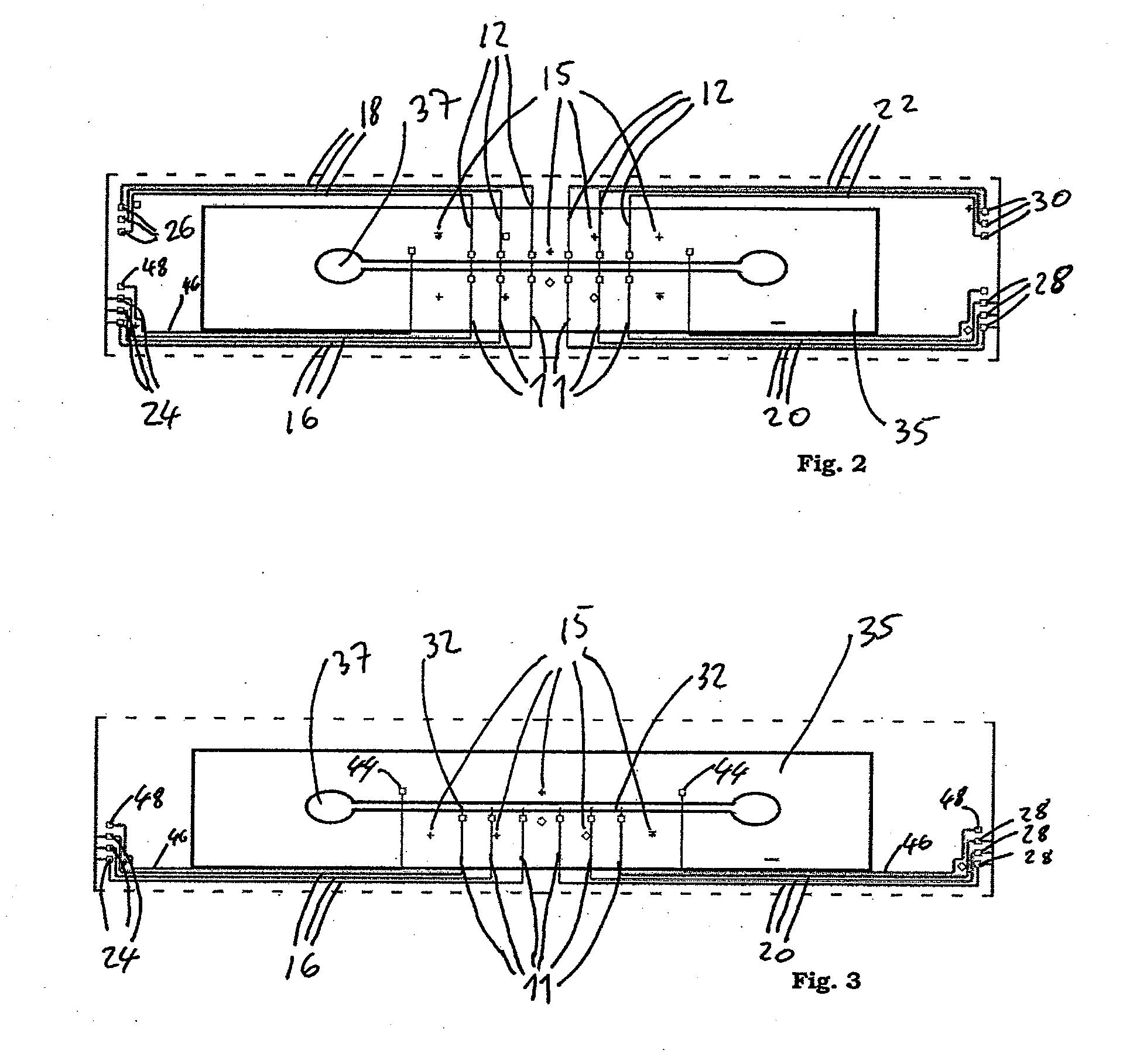
[0017]An apparatus or a chip of this kind is particularly suited for automatic detection of analytes on an industrial scale. Each FET formed by a pair of first and second electrodes and the associated elongate nanostructure can be designed to detect a specific analyte or a plurality of different analytes if an appropriate number of suitably functionalized elongate nanostructures are provided for each pair of electrodes. When plural FETs are provided each can be designed for detecting the same analyte or plurality of analytes. Alternatively, the individual FETs or groups of them can be designed for detecting different analytes or different pluralities of analytes. The corresponding substrate or chip bearing the array of FETs can be positioned beneath an automatic dispenser for samples for investigation, a so-called spotter, and the spotter can be operated to dispense a drop of the sample or samples into the respective wells. This process can take place under computer control so that there is a unique association between each sample and the FETs on the chip and an equally unique and unambiguous association between the detector readouts and the individual FETs. Furthermore, the reference electrode or electrodes facilitate rapid and unambiguous calibration of the apparatus and of the detection result.
[0019]Whereas, in the prior art, the readout of the impedance values has been realized as a DC readout, it has been found that a measurement of the complex resistance, i.e. with respect to both magnitude and phase, leads to a much higher sensitivity which contributes significantly to the desired sensitivity of detection of analytes, i.e. makes it possible to reliably detect even lower concentrations of analytes.

Problems solved by technology

The problem with all existing detectors is that their sensitivity still leaves scope for improvement.

Method used


Image

  • Apparatus and method for detecting one or more analytes
  • Apparatus and method for detecting one or more analytes
  • Apparatus and method for detecting one or more analytes

Examples


Embodiment Construction

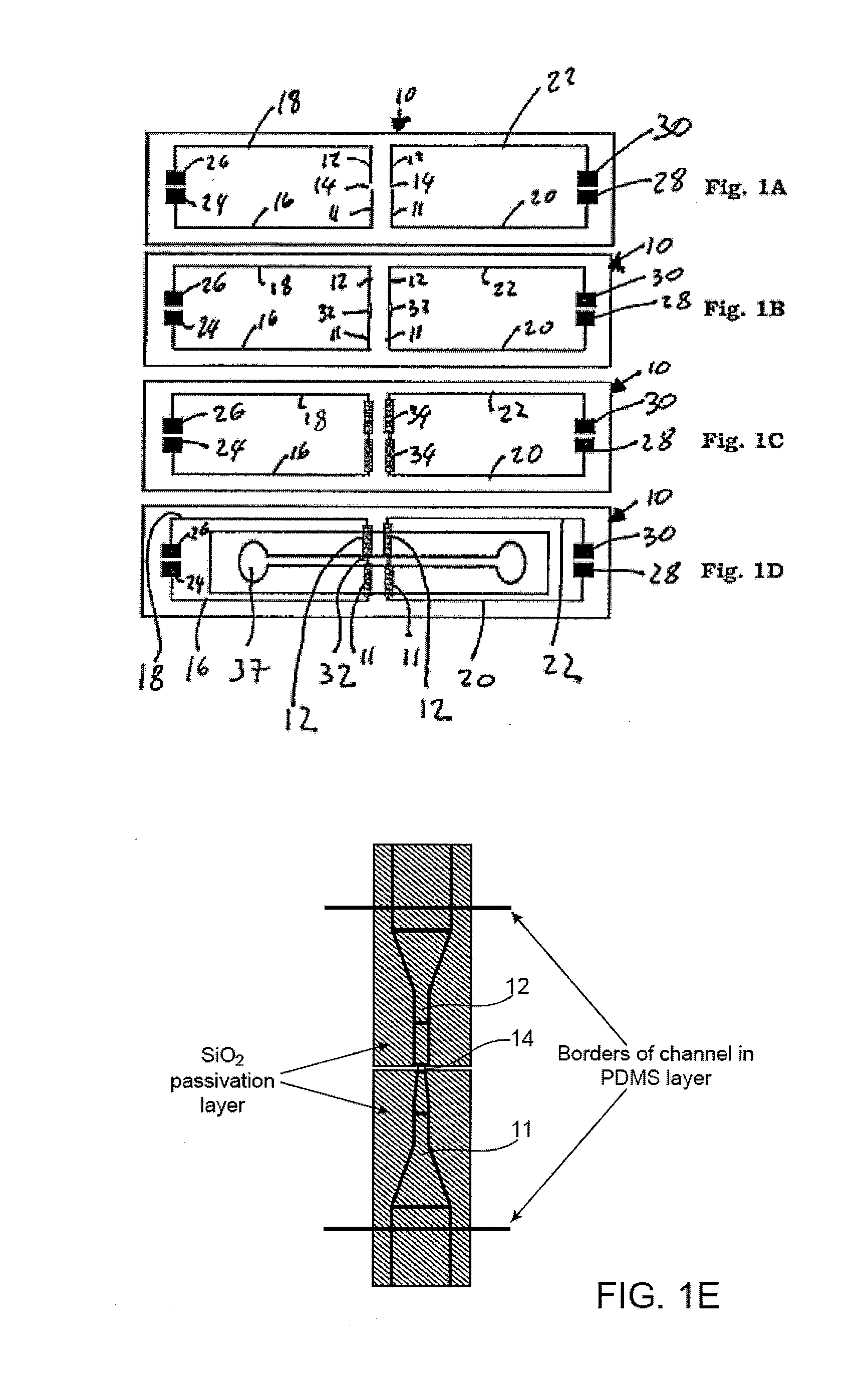
[0054]General Description of Detector Topographies and their Manufacture

[0055]Turning now to FIG. 1A there can be seen a substrate 10 which can, for example, consist of a material selected from the group comprising glass, polyimide, silicon / silicon oxide, quartz and silicon nitride. In the present case the substrate 10 consists of an insulating silicon dioxide layer of 500 nm thickness which is an insulator on an n+-type substrate of crystalline Si with a resistivity of 1 Ohm / cm2 and of 500 μm thickness.

[0056]It should be noted that reference in the specification to silicon oxide means SiOx, where x can have values between 1 and 2 and signifies a non-stoichiometric oxide. However, SiO2, i.e. Silicon dioxide, is a perfectly viable and extremely useful silicon oxide for the purposes of the present invention, both as an insulating layer on a conductive silicon substrate and as a passivation layer.

[0057]Two pairs of first and second electrodes 11 and 12 of, in this case, platinum are de...


PUM

PropertyMeasurementUnit
Timeaaaaaaaaaa
Nanoscale particle sizeaaaaaaaaaa

Abstract

The present invention relates to an apparatus for detecting one or more analytes, for example analytes selected from the group comprising nucleic acids, metabolites, peptides, proteins, hormones, pesticides, neurotransmitters, ions in blood, electrolytes, toxic gases, pH and biological warfare agents, the apparatus comprising an insulating substrate, at least one first electrode on the substrate at least one elongate nanostructure extending from and electrically connected to the or each said electrode and extending over the surface of the wafer away from the respective electrode, a passivating layer covering the or each electrode, but not all of said at least one elongate nanostructure, a well crossing the at least one elongate nanostructure extending from the or each electrode and forming a static reservoir for a liquid being investigated for the presence of at least one analyte, a reference electrode provided on said substrate within said well or insertable into said well and respective readout pads electrically connected to the or each electrode and to the reference electrode if the latter is provided on the substrate, the at least one elongate nanostructure being capable of being functionalized for detecting one or more analytes.

Description

CROSS-REFERENCES TO RELATED APPLICATIONS[0001]This application claims priority to European Applications Nos. 10 009 053.9, filed Aug. 31, 2010, and 10 012 585.5, filed Sep. 30, 2010, the disclosures of both of which are incorporated herein by reference.BACKGROUND OF THE INVENTION[0002]The present invention relates to an apparatus and to a method of fabricating an apparatus for detecting one or more analytes, for example analytes selected from the group comprising nucleic acids, metabolites, peptides, proteins, and hormones, the apparatus comprising an insulating substrate, at least one first electrode on the substrate, at least one elongate nanostructure extending from and electrically connected to the or each electrode and extending over the surface of the wafer away from the respective electrode.[0003]An apparatus of this general kind and realized as an FET is known from the document “Label-Free DNA Biosensors Based on Functionalized Carbon Nanotube Field Effect Transistors” by Ma...

Claims


Application Information

Patent Timeline
IPC IPC(8): G01N27/02B05D7/00C25D15/00C23C28/00B05D5/12C25D15/02B82Y15/00
CPCB82Y15/00G01N27/127G01N27/4146G01N27/4145G01N27/128G01N21/554G01N33/487G01N21/6489
Inventor KURKINA, TETIANAVLANDAS, ALEXISRAFIEFARD, NASSIMAHMAD, ASHRAFKERN, KLAUSBALASUBRAMANIAN, KANNAN
Owner MAX PLANCK GESELLSCHAFT ZUR FOERDERUNG DER WISSENSCHAFTEN EV
Learn More