

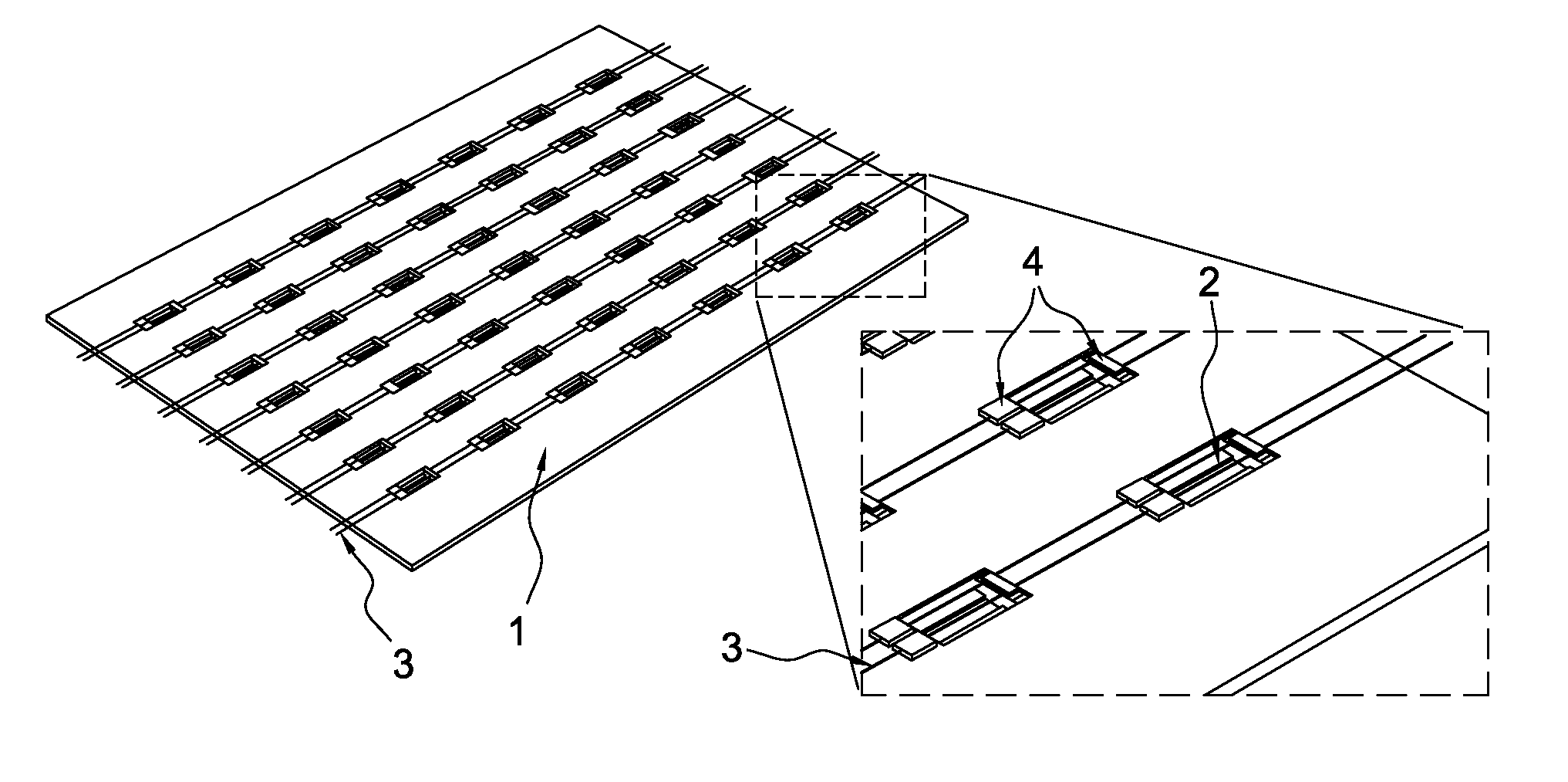
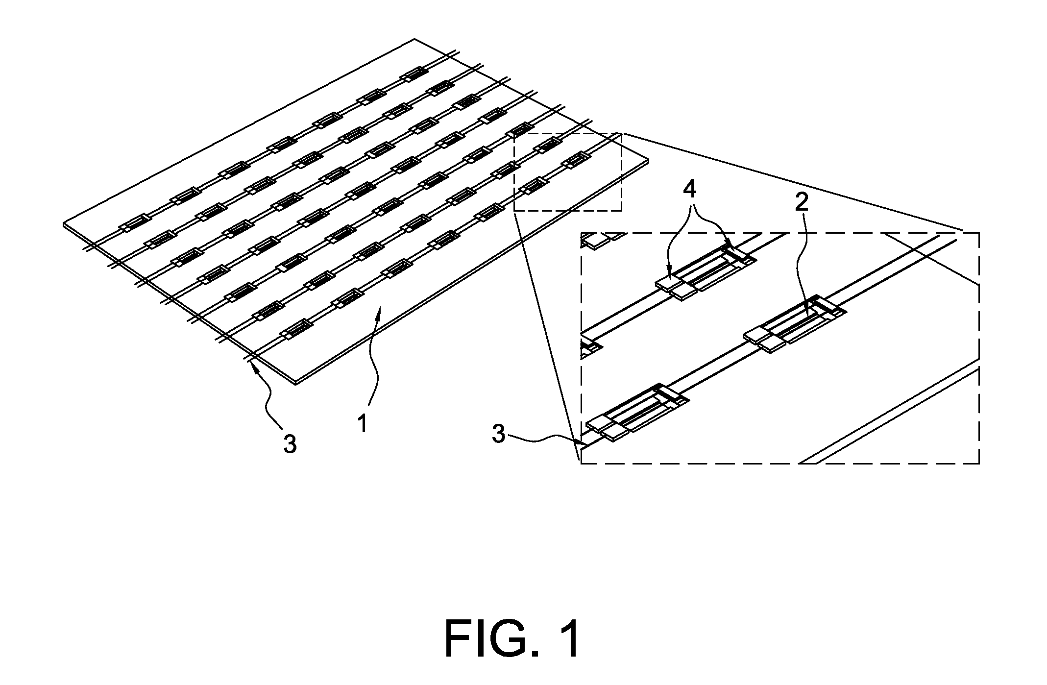
Method for mechanical and electrical integration of sma wires to microsystems
a technology of mechanical and electrical integration and microsystems, applied in the field of microsystems, can solve the problems of sma wire success, affecting work, and affecting the success of sma in micro-electro-mechanical systems (mems), and achieves cost-efficient and robust integration methods
- Summary
- Abstract
- Description
- Claims
- Application Information
AI Technical Summary
Benefits of technology
Problems solved by technology
Method used
Image

Examples
examples
[0108]An array of actuators according to an embodiment of the present invention shown in FIG. 5 was fabricated from a silicon substrate at wafer scale and tested. The total footprint of each device was 4.5×1.8 mm2.
[0109]Repeatable actuation was observed, and the actuator featured deflections between 80 μm and 540 μm, thus a net stroke of 460 μm. The actuation current at full deflection was 82 mA, for a corresponding voltage of about 0.8 V, hence a maximum input power below 70 mW. FIG. 6 shows the actuator deflection vs. input power along a complete heating-cooling cycle during testing of a sample.
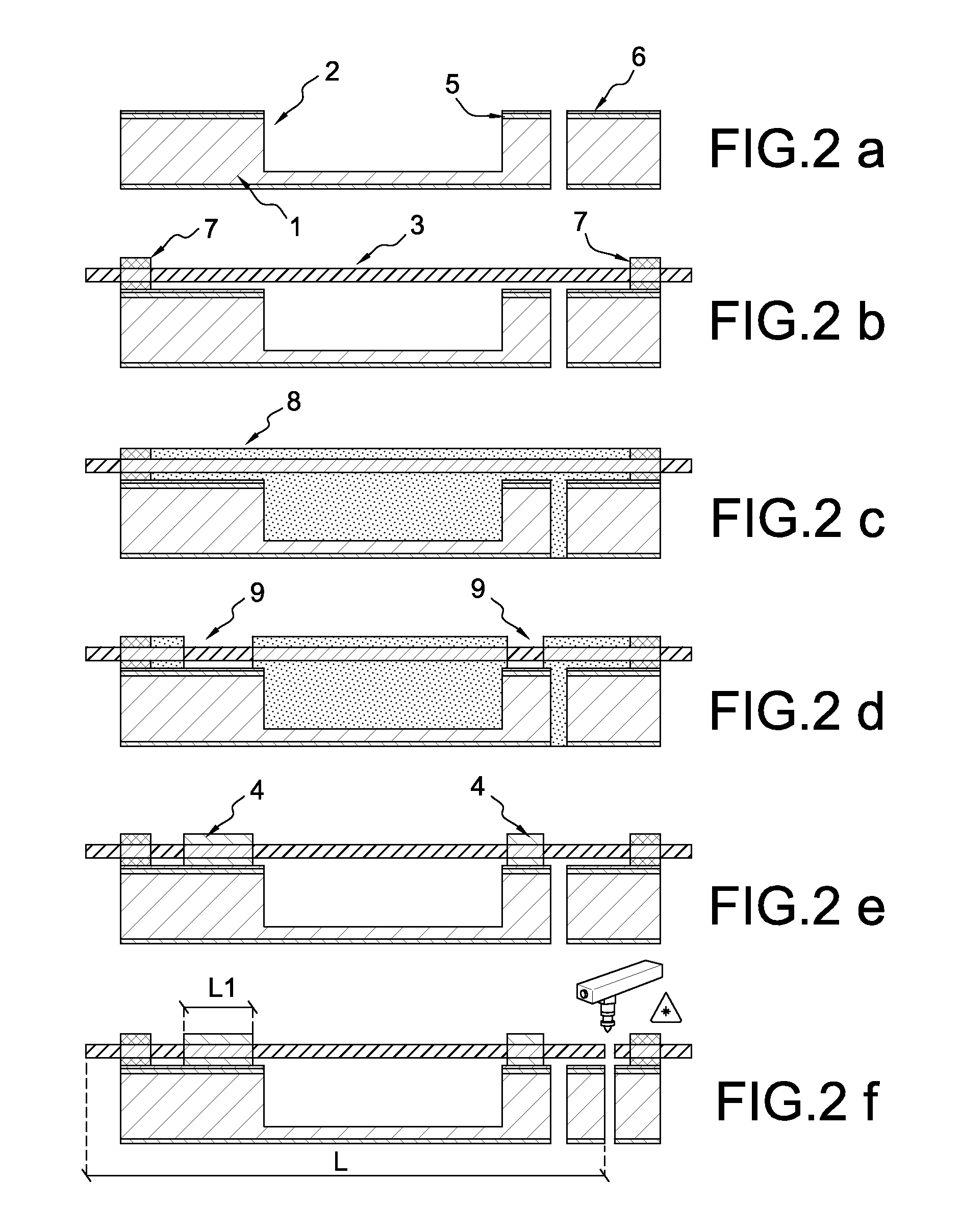
[0110]The bond between the SMA wires and the electroplated nickel on test structures fabricated according to the present invention was investigated by scanning electron microscopy (SEM) and by mechanical testing using a tool for wire bonding testing (Dage PC 2400).
[0111]Prior to the SEM, a chip was embedded in polymer for mechanical stability, then a cross-section of the electroplated fixtu...
PUM
| Property | Measurement | Unit |
|---|---|---|
| thicknesses | aaaaa | aaaaa |
| thickness | aaaaa | aaaaa |
| thickness | aaaaa | aaaaa |
Abstract
Description
Claims
Application Information