Tunnel field effect transistor and method for manufacturing same

a technology of tunneling field and transistor, which is applied in the direction of nanotechnology, crystal growth process, polycrystalline material growth, etc., can solve the problems of increased power consumption, increased power consumption, and increased power consumption, so as to improve the integration and performance suppress the increase in power consumption of a large-scale integrated circuit, and facilitate the manufacture of a tfet

Active Publication Date: 2012-07-26
HOKKAIDO UNIVERSITY
View PDF2 Cites 52 Cited by
  • Summary
  • Abstract
  • Description
  • Claims
  • Application Information

AI Technical Summary

Benefits of technology

[0037]The present invention can easily manufacture a TFET (switch element) that can operate at a small subthreshold (60 mV/digit or below). Using the TFET of the present invention makes it possible to improve a degree of in

Problems solved by technology

One of problems when reducing the size of the CMOS is an increase of power consumption.
An increase in the number of CMOSs that can be mounted on one microchip and an increase of leakage current caused by a short channel effect can be cited as two of the maj

Method used


Image

  • Tunnel field effect transistor and method for manufacturing same
  • Tunnel field effect transistor and method for manufacturing same
  • Tunnel field effect transistor and method for manufacturing same

Examples


embodiment 1

[0107]Embodiment 1 will show an example of a TFET of the present invention manufactured using a silicon (111) substrate high doped to be a p-type.

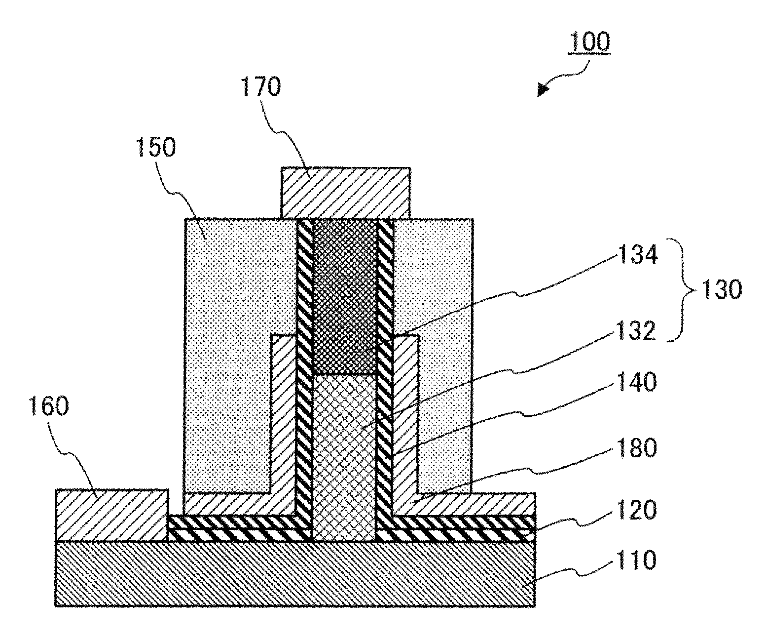
[0108]FIG. 4 is a cross-sectional view showing a configuration of the TFET according to Embodiment 1. As shown in FIG. 4, TFET 100 of Embodiment 1 includes high p-type doped silicon substrate 110, insulating film 120, group III-V compound semiconductor nanowire 130, gate dielectric film 140, insulating protective film 150, source electrode 160, drain electrode 170 and gate electrode 180. Group III-V compound semiconductor nanowire 130 is made up of undoped first region 132 and high n-type doped second region 134.

[0109]Silicon substrate 110 is a high p-type doped silicon (111) substrate.

[0110]Insulating film 120 is an insulating film that covers a surface ((111) surface) of the two surfaces of p-type silicon substrate 110 on which at least group III-V compound semiconductor nanowire 130 is arranged. Insulating film 120 is a silicon oxide (S...

embodiment 2

[0119]Embodiment 2 shows an example of TFET according to the present invention manufactured using a high n-type doped silicon (111) substrate.

[0120]FIG. 7 is a cross-sectional view showing a configuration of the TFET according to Embodiment 2. Configuration elements identical to those of the TFET of Embodiment 1 are assigned the same reference numerals, and duplicate descriptions thereof are omitted.

[0121]As shown in FIG. 7, TFET 200 of Embodiment 2 includes high n-type doped silicon substrate 210, insulating film 120, group III-V compound semiconductor nanowire 220, gate dielectric film 140, insulating protective film 150, source electrode 160, drain electrode 170 and gate electrode 180. Group III-V compound semiconductor nanowire 220 is constructed of low n-type doped first region 222 and high p-type doped second region 224.

[0122]Silicon substrate 210 is a high n-type doped silicon (111) substrate.

[0123]Group III-V compound semiconductor nanowire 220 is a nanowire made of group II...

embodiment 3

[0125]Embodiment 3 shows an example of a TFET according to the present invention manufactured using a low p-type doped silicon (100) substrate.

[0126]FIG. 9 is a cross-sectional view showing a configuration of the TFET of Embodiment 3. As shown in FIG. 9, TFET 300 of Embodiment 3 includes low p-type doped silicon substrate 310, low p-type doped group III-V compound semiconductor nanowire 320, insulating film (gate dielectric film) 330, source electrode 340, drain electrode 350 and gate electrode 360. Part of the region of insulating film 330 also functions as a gate dielectric film. P-type silicon substrate 310 includes undoped first region 312 and high n-type doped second region 314.

[0127]Silicon substrate 310 is a low p-type doped silicon (100) substrate. Undoped first region 312 (intrinsic semiconductor) and high n-type doped second region 314 (n-type semiconductor) are arranged so as to neighbor each other on the surface out of the two surfaces of silicon substrate 310 on which g...


PUM

PropertyMeasurementUnit
Currentaaaaaaaaaa
Digital informationaaaaaaaaaa
Temperatureaaaaaaaaaa

Abstract

A tunnel field effect transistor is capable of operating at a low subthreshold and is able to be manufactured easily. The tunnel field effect transistor includes a group IV semiconductor substrate having a (111) surface and doped so as to have a first conductivity type, a group III-V compound semiconductor nanowire arranged on the (111) surface and containing a first region connected to the (111) surface and a second region doped so as to have a second conductivity type, a source electrode connected to the group IV semiconductor substrate; a drain electrode connected to the second region, and a gate electrode for applying an electric field to an interface between the (111) surface and the group III-V compound semiconductor nanowire, or an interface between the first region and the second region.

Description

TECHNICAL FIELD[0001]The present invention relates to a tunnel field effect transistor including a group III-V compound semiconductor nanowire and a manufacturing method thereof.BACKGROUND ART[0002]Semiconductor microprocessors and large scale integrated circuits are manufactured by integrating elements such as metal-oxide-semiconductor (hereinafter referred to as “MOS”) field effect transistor (hereinafter referred to as “FET”) on a semiconductor substrate. Complementary MOSFETs (hereinafter referred to as “CMOS”) are generally basic elements (switch elements) of such integrated circuits. As the material for semiconductor substrates, silicon which is group IV semiconductor is mainly used. The degree of integration and performance of semiconductor microprocessors and large scale integrated circuits can be improved by reducing the size of transistors making up a CMOS. One of problems when reducing the size of the CMOS is an increase of power consumption. An increase in the number of ...

Claims


Application Information

Patent Timeline
IPC IPC(8): H01L29/775H01L21/20B82Y40/00B82Y99/00
CPCB82Y10/00B82Y40/00C23C16/45525H01L21/02373H01L21/02381H01L21/02433H01L21/02538H01L21/02546H01L21/02603H01L21/02609H01L29/045H01L29/0665H01L29/267H01L29/66356H01L29/7391C30B25/005C30B25/186C30B29/40C23C16/303C30B29/62H01L21/20H01L21/326H01L29/06H01L29/12H01L29/66H01L29/772H01L29/78
Inventor TOMIOKA, KATSUHIROFUKUI, TAKASHITANAKA, TOMOTAKA
Owner HOKKAIDO UNIVERSITY
Why Eureka
Try Eureka