
Microwave plasma electron flood

a plasma electron flood and microwave technology, applied in the field of plasma electron flood, can solve the problems of gate oxide damage, low yield of wafers, and low ratio of wafers implanted with desired properties to total wafers, and achieve the effect of low magnetic field strength and high magnetic field strength

Active Publication Date: 2012-07-26
AXCELIS TECHNOLOGIES
View PDF6 Cites 7 Cited by
  • Summary
  • Abstract
  • Description
  • Claims
  • Application Information

AI Technical Summary

Benefits of technology

[0006]The present invention is directed towards a method and apparatus for generating a plasma electron flood (PEF) using microwave radiation. In one embodiment, the apparatus comprises a microwave PEF apparatus having one or more permanent magnets configured to generate a magnetic field that rapidly decays over a cavity (e.g., PEF cavity), resulting in a static magnetic field having a high magnetic field strength (typically 2 kGauss-4 kGauss) near one side (e.g., the “bottom”) of the cavity and a low magnetic field strength (e.g., a substantially zero magnetic field) near the opposite side (e.g., the “top”) of the cavity, which comprises an extraction aperture (e.g., an elongated extraction slit) in direct communication with an ion beamline. In one particular embodiment, the one or more permanent magnets are located at a position (e.g., at the “bottom” of the PEF cavity) that is spatially opposed to the location of the extraction aperture to achieve the rapidly decaying magnetic field. The magnetic field results in an electron cyclotron frequency in a region of the cavity that is equal to or approximately equal to a microwave radiation frequency so that a plasma is generated to diffuse through the extraction aperture.

Problems solved by technology

If these non-uniformities are not corrected the workpiece may be implanted non-uniformly and wafer yield (i.e. the ratio of wafer area implanted with desired properties to total wafer area) may suffer.
This effect, commonly referred to as charging, can be detrimental to the semiconductor circuit if the voltages of the insulated feature (e.g. the gate electrode) exceed the breakdown voltage of the insulator (e.g. the gate oxide) such that resultant damage to the gate oxide occurs.
It can be appreciated that the charging rate and voltage increase with beam current, and that ion implantation with ever increasing beam currents represents an increasing processing challenge.

Method used


Image

  • Microwave plasma electron flood
  • Microwave plasma electron flood
  • Microwave plasma electron flood

Examples


Embodiment Construction

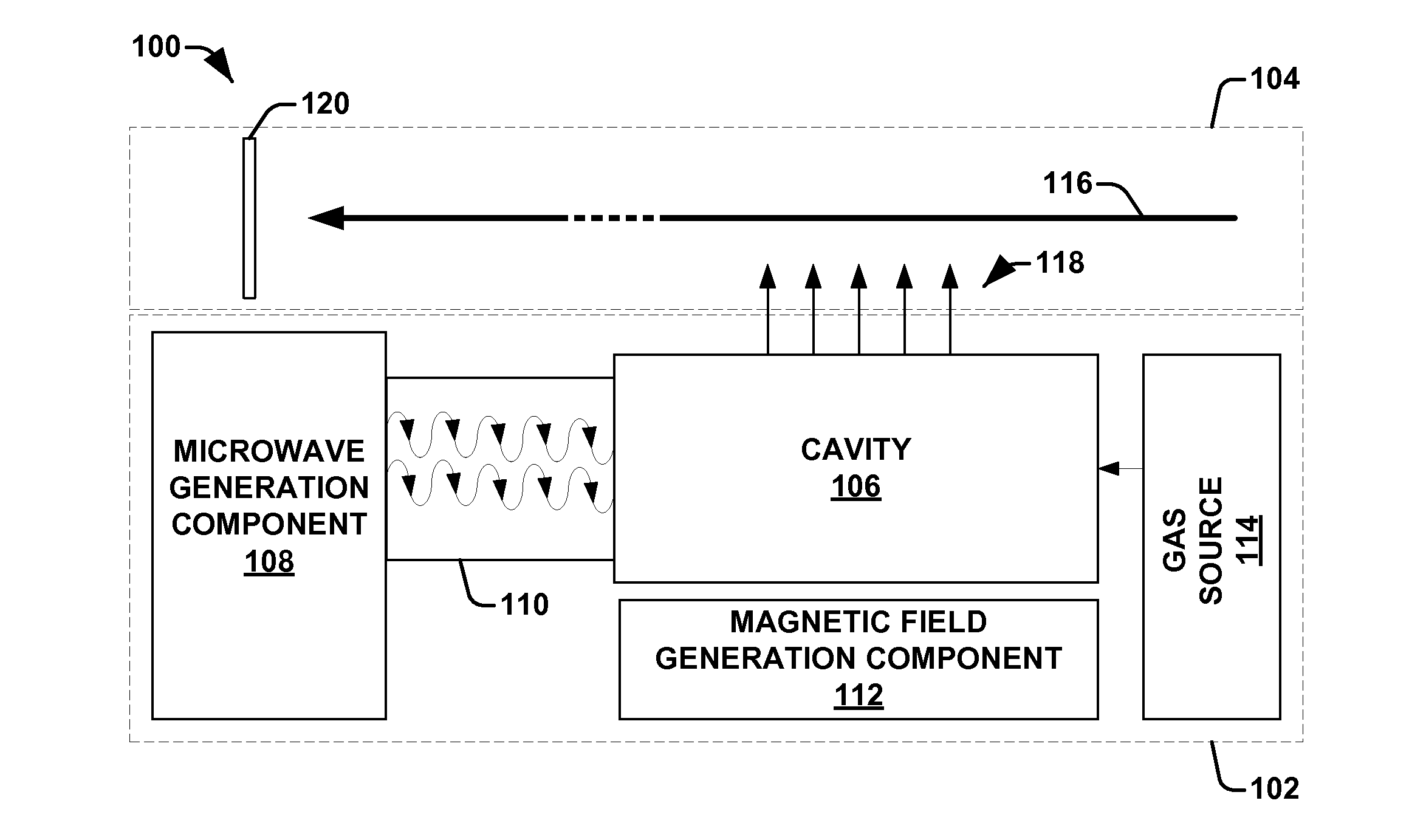
[0017]The present invention will now be described with reference to the drawings wherein like reference numerals are used to refer to like elements throughout.

[0018]The electron flood apparatus is an important subsystem of ion implanters. The electron flood apparatus provides neutralizing charged particles into a beamline comprising an ion beam to generate an ion beam having an overall charge neutrality. Charge neutrality allows for reduction of costs associated with integrated chip fabrication by improving the uniformity of ion beam implantation over a wafer and by avoiding damage due to the charging of insulated wafer components.

[0019]Generally, a plasma electron flood apparatus have generated a plasma, comprising a DC discharge that is produced from a hot cathode that emits electrons to ionize neutral gas atoms introduced into a PEF. However, due to cathode life limitations, periodic maintenance is required, increasing operational costs and ion implanter down time. Furthermore, t...


PUM


Abstract

A method and apparatus is provided for generating a plasma electron flood using microwave radiation. In one embodiment, a microwave PEF apparatus is configured to generate a magnetic field that rapidly decays over a PEF cavity, resulting in a static magnetic field having a high magnetic field strength near one side (e.g., “bottom”) of the PEF cavity and a low magnetic field strength (e.g., substantially zero) near the opposite side (e.g., “top”) of the PEF comprising an elongated extraction slit. In one particular embodiment, the one or more permanent magnets are located at a position that is spatially opposed to the location of the elongated extraction slit to achieve the rapidly decaying magnetic field.The magnetic field results in an electron cyclotron frequency in a region of the cavity equal to or approximately equal to a microwave radiation frequency so that plasma is generated to diffuse through the extraction apertures.

Description

FIELD OF THE INVENTION[0001]The present invention relates generally to ion implantation systems, and more specifically to a method and apparatus for producing a plasma electron flood.BACKGROUND OF THE INVENTION[0002]In the manufacture of semiconductor devices, ion implantation is often used to dope semiconductor workpieces (e.g., silicon wafers) with impurities. For example, ion implanters or ion implantation systems may treat a workpiece with an ion beam to produce n-type or p-type doped regions or to form passivation layers on the workpiece. When used for doping semiconductors, the ion implantation system may inject a selected ion species to produce a desired extrinsic material.[0003]In general, in ion implantation systems, maintaining an ion beam having charge neutrality (e.g., forming an ion beam plasma having a substantially equal density of both positively charged and negatively charged particles) is important for producing a high quality ion implantation. Charge neutrality ai...

Claims


Application Information

Patent Timeline
Patent Type & Authority Applications(United States)
IPC IPC(8): H05H1/46
CPCH01J37/026H05H2001/4622H05H1/46H01J37/3171H05H1/4622
Inventor DIVERGILIO, WILLIAM F.VANDERBERG, BO
Owner AXCELIS TECHNOLOGIES
Learn More