Film forming method, semiconductor device manufacturing method, insulating film and semiconductor device

Inactive Publication Date: 2012-07-26
TOKYO ELECTRON LTD
View PDF3 Cites 7 Cited by
  • Summary
  • Abstract
  • Description
  • Claims
  • Application Information

AI Technical Summary

Benefits of technology

[0029]In accordance with a film forming method of illustrative embodiments, even if a processing target substrate has a shape having a high aspect ratio or a microscopic stepped portion, it is possible to form a film so as to cover the shape completely by forming a adsorption layer on the processing target substrate by adsorbing a film forming gas on the processing target substrate. Further, since a plasma process is performed by microwave plasma, plasma damage can be greatly reduced in a film forming process. Accordingly, in accordance

Problems solved by technology

However, if a silicon oxide having high insulation property is formed by the th

Method used


Image

  • Film forming method, semiconductor device manufacturing method, insulating film and semiconductor device
  • Film forming method, semiconductor device manufacturing method, insulating film and semiconductor device
  • Film forming method, semiconductor device manufacturing method, insulating film and semiconductor device

Examples


Embodiment Construction

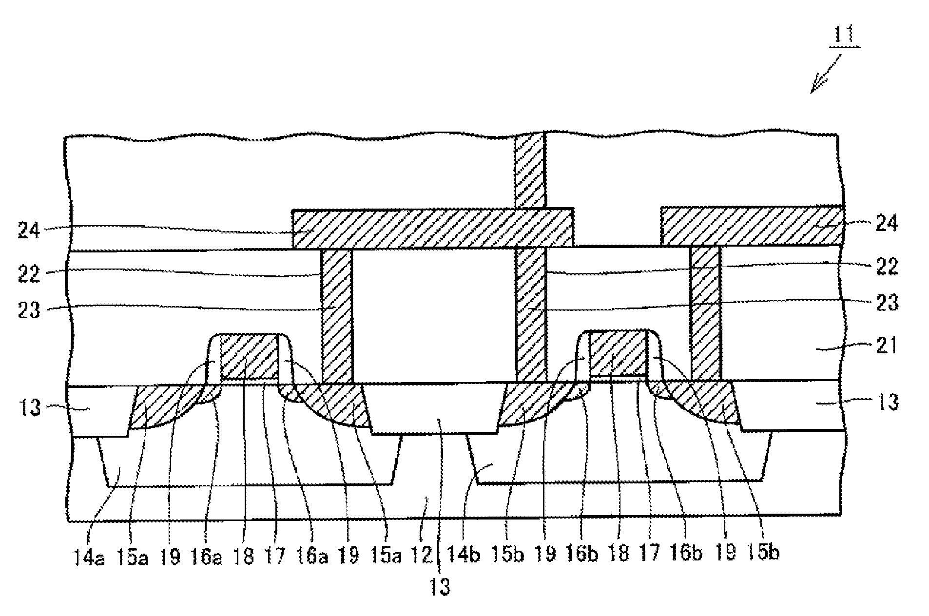
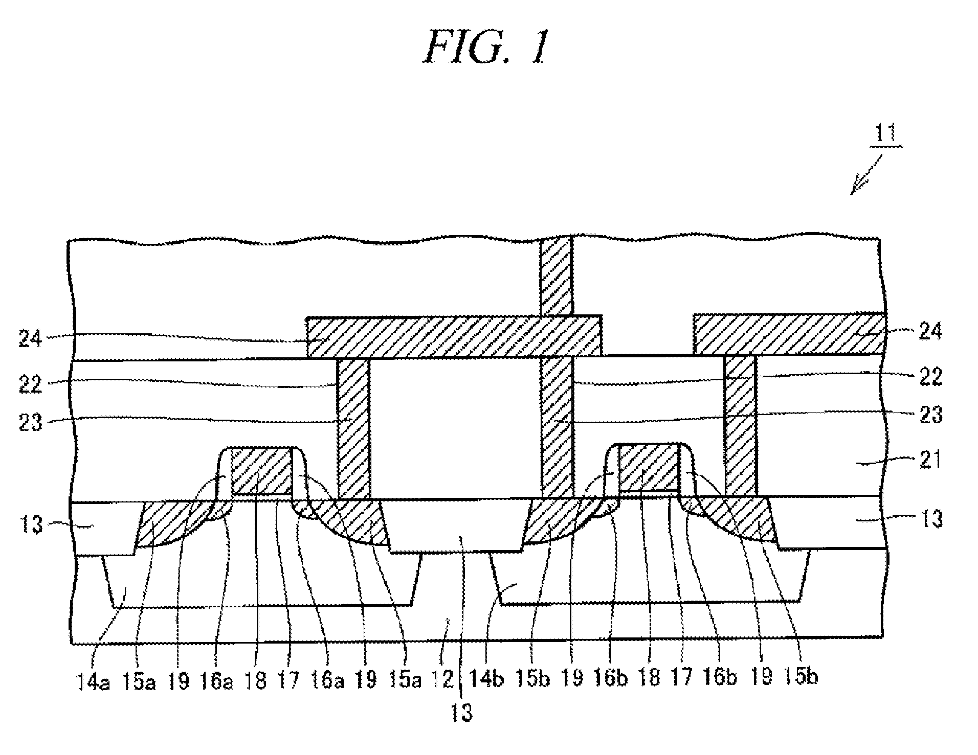
[0054]Hereinafter, illustrative embodiments will be described with reference to the accompanying drawings. First, a structure of a semiconductor device in accordance with an illustrative embodiment will be explained. FIG. 1 is a schematic cross sectional view illustrating a part of a MOS semiconductor device in accordance with an illustrative embodiment. In FIG. 1, a conductive layer of the MOS semiconductor device is hatched.

[0055]Referring to FIG. 1, a MOS semiconductor device 11 includes, a silicon substrate 12 on which device isolation regions 13, p-wells 14a, n-wells 14b, high-concentration n-type impurity diffusion regions 15a, high-concentration p-type impurity diffusion regions 15b, n-type impurity diffusion regions 16a, p-type impurity diffusion regions 16b and gate oxide films 17 are provided. One of the high-concentration n-type impurity diffusion regions 15a and the high-concentration p-type impurity diffusion regions 15b provided with the gate oxide films 17 therebetwee...


PUM

PropertyMeasurementUnit
Pressureaaaaaaaaaa
Pressureaaaaaaaaaa
Energyaaaaaaaaaa

Abstract

In a film forming method, firstly, a processing target substrate W as a base of a semiconductor device is held on a mounting table 34 by an electrostatic chuck. Then, a film forming gas is adsorbed onto the processing target substrate W (a gas adsorption process) ((A) of FIG. 6). Thereafter, the inside of the processing chamber 32 is evacuated in order to remove residues of the film forming gas ((B) of FIG. 6). Upon the completion of the first exhaust process, a plasma process using microwave is performed ((C) of FIG. 6). Upon the completion of the plasma process, the inside of the processing chamber 32 is evacuated in order to remove an unreacted reactant gas and the like ((D) of FIG. 6). These series of steps (A) to (D) are repeated in this sequence until a desired film thickness is obtained.

Description

TECHNICAL FIELD[0001]The present disclosure relates to a film forming method, a semiconductor device manufacturing method, an insulating film and a semiconductor device. More particularly, the present disclosure relates to a semiconductor device manufacturing method and a film forming method using a plasma process, and also relates to a semiconductor device and an insulating film formed by the plasma process.BACKGROUND ART[0002]Conventionally, when forming an insulating layer having high pressure resistance property or excellent leak property against a gate oxide film of a semiconductor device represented as a LSI (Large Scale Integrated circuit), a CCD (Charge Coupled Device) or a MOS (Metal Oxide Semiconductor) transistor, a thermal CVD (Chemical Vapor Deposition) method is generally used. However, if a silicon oxide having high insulation property is formed by the thermal CVD method, a silicon substrate needs to be exposed to a high temperature. In this case, if a conductive laye...

Claims


Application Information

Patent Timeline
IPC IPC(8): H01L21/31H01L21/30
CPCC23C16/345C23C16/401C23C16/45542H01L21/02164H01L29/66181H01L21/02274H01L21/0228H01L21/28194H01L21/0217C23C16/44H01L21/205
Inventor UEDA, HIROKAZUOHSAWA, YUSUKEHORIGOME, MASAHIRO
Owner TOKYO ELECTRON LTD
Why Eureka
Try Eureka