Ultrananocrystalline Diamond Films with Optimized Dielectric Properties for Advanced RF MEMS Capacitive Switches

a capacitive switch and diamond film technology, applied in electronic switching, relays, pulse techniques, etc., can solve the problems of lack of reliability, limited acceptance in the industry, and main limitation of lifetime of dielectric charging, so as to achieve reliable, effective and efficient

Active Publication Date: 2012-08-02
UCHICAGO ARGONNE LLC
View PDF3 Cites 5 Cited by
  • Summary
  • Abstract
  • Description
  • Claims
  • Application Information

AI Technical Summary

Benefits of technology

[0016]An improved RF MEMS capacitive switch and fabrication process therefore is provided for use in controlling, routing, and tuning RF wireless circuits and systems, as well as for other uses and applications. Advantageously, the improved RF MEMS capacitive switch is reliable, effective and efficient. Significantly,

Problems solved by technology

Despite the excellent RF performance of these devices, their acceptance in industry has been limited by a lack of reliability.
In a well-engineered MEMS switch, dielectric charging is the main limitation to lifetime, as opposed to mechanical effects.
If enough charges become trapped, the operating voltages will shift sufficiently such that the switch will either remain stuck down, or not actuate when desired.
In either case, the switch fails to operate properly.
Furthermore, while the RF performance of these devices can be exemplary, reliability issues have limited their deployment into fielded systems, in the case of capacitive MEMS switches, shortcomings relating to dielectric charging have been difficult to mitigate.
These solutions have provided significant improvements in reliability, but have not proven enough to overcome the “stigma” associated with dielectric charging.
Charges become trapped in the layer and charge builds over time.
As the charge builds, the operation of the device degrades until it fails.
In fact, it fails very slowly.
After failure, a device may take days to recover because charges trapped in the dielectric layer take so long to recombine at the metal electrodes of the capacitor.
Furthermore, the higher the operating temperature, generally the faster the switch will fail.
Conventional prior switches slowly degrade until the point of failure.
Therefore, once failure has occurred, conventional prior art devices are not available for proper operation for a very long time period, rendering the device essentially useless for a majority of applications and uses.
The primary failure mode of conventional prior art RF MEMS capacitive switches is accumulation of electrically charged particles within the insulator layer made of silicon oxide or silicon nitride materials of the switch, in which charges tunnel into and become trapped within the dielectric.
The conventional prior art RF MEMS capacitive switch only recovers from this failure after a sufficiently long perio

Method used


Image

  • Ultrananocrystalline Diamond Films with Optimized Dielectric Properties for Advanced RF MEMS Capacitive Switches
  • Ultrananocrystalline Diamond Films with Optimized Dielectric Properties for Advanced RF MEMS Capacitive Switches
  • Ultrananocrystalline Diamond Films with Optimized Dielectric Properties for Advanced RF MEMS Capacitive Switches

Examples


Embodiment Construction

[0067]The following is a detailed description and explanation of the preferred embodiments of the invention and best modes for practicing the invention.

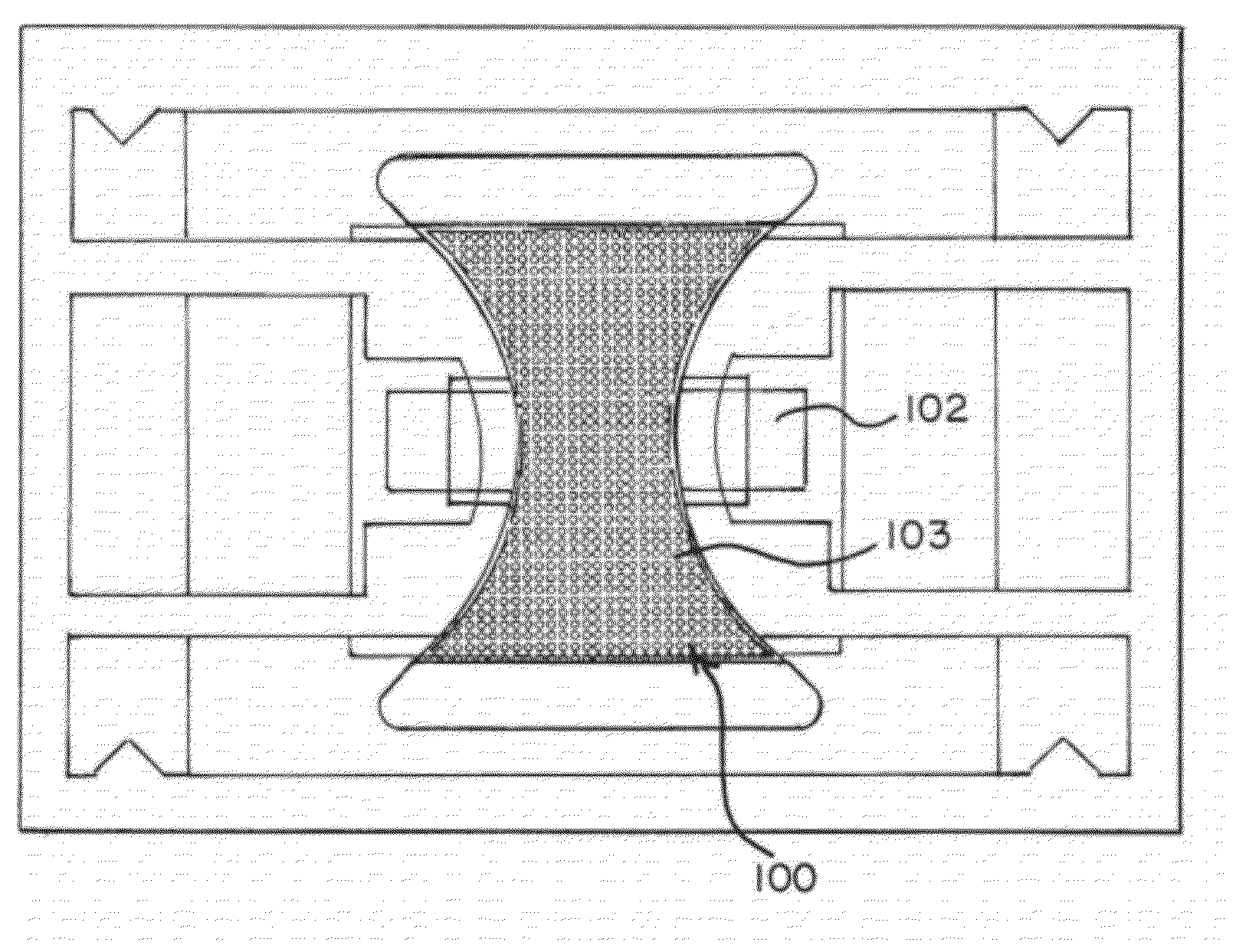
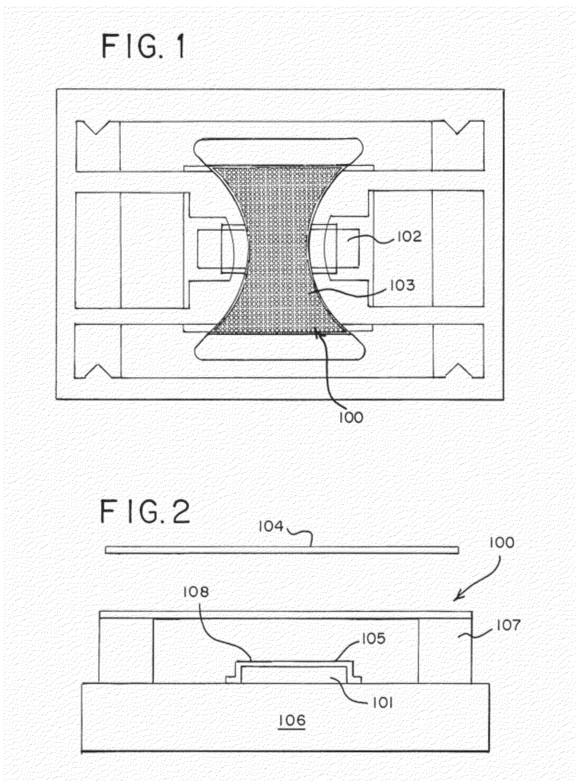
[0068]Referring to the drawings, a radio frequency (RF) microelectromechanical (MEMS) capacitive switch 100 (FIGS. 1 and 2) is moveable for a switching time from an off position in an off state to an on position in an on state. The RF MEMS capacitive switch can have: a bottom electrode 102 comprising metal that provides a RF signal path; a top electrode 104 comprising an RF ground and a direct current (DC) ground; a moveable metallic membrane 106, and multiple layered (multi-layered) dielectric films 108 with electrical leaky characteristics and providing multiple dielectric insulating layers on the bottom electrode. The RF MEMS capacitive switch can also have undercut access holes 110. The RF MEMS capacitive switch can have a substrate 112, such as a silicon on sapphire (SOS) substrate 114, positioned below the bottom electrode and ...


PUM

PropertyMeasurementUnit
Temperatureaaaaaaaaaa
Timeaaaaaaaaaa
Lengthaaaaaaaaaa

Abstract

An efficient deposition process is provided for fabricating reliable RF MEMS capacitive switches with multilayer ultrananocrystalline (UNCD) films for more rapid recovery, charging and discharging that is effective for more than a billion cycles of operation. Significantly, the deposition process is compatible for integration with CMOS electronics and thereby can provide monolithically integrated RF MEMS capacitive switches for use with CMOS electronic devices, such as for insertion into phase array antennas for radars and other RF communication systems.

Description

STATEMENT REGARDING FEDERALLY SPONSORED RESEARCH OR DEVELOPMENT[0001]The United States Government has rights in this invention pursuant to Contract No. DE-ACO2-06CH11357 between the U.S. Department of Energy (DOE) and UChicago Argonne, LLC representing Argonne National Laboratory and pursuant to Contract No, MIPR06-W238 between the Defense Advanced Research Projects Agency (DARPA) and UChicago Argonne, LLC representing Argonne National Laboratory.BACKGROUND OF THE INVENTION[0002]This invention relates to capacitive switches and more particularly, to radio frequency (RF) microelectromechanical systems (MEMS) capacitive switches and a fabrication process therefore.[0003]RF MEMS capacitive switches have many useful applications for military and commercial RF and microwave applications, RF MEMS capacitive switch comprises a movable metal membrane suspended above a lower electrode and an interposing dielectric layer. An air gap of several microns typically separates the upper membrane fr...

Claims


Application Information

Patent Timeline
IPC IPC(8): H01L27/20H01L21/77B82Y15/00B82Y40/00
CPCB82Y30/00H01H59/0009Y10T29/49105H01L27/13B82Y40/00H10N39/00H01H2059/0081H01H2209/014H01H2209/046H01H2209/07H01H2239/004H01H2239/006H03K17/975
Inventor SUMANT, ANIRUDHA V.AUCIELLO, ORLANDO H.MANCINI, DERRICK C.
Owner UCHICAGO ARGONNE LLC
Why Eureka
Try Eureka