This helps you quickly interpret patents by identifying the three key elements:
Problems solved by technology
Method used
Benefits of technology
[0020]The precursors or gases in NLD process are not limited to only those having the self-limiting surface reactions since NLD is a deposition process. NLD thus is precursor-dependent and can be used to deposit a vast number of film materials from currently available precursors. Since NLD process has high throughput, the minimal volume constraint as in ALD process is not necessary, and conventional CVD chamber can be used to achieve highly conformal, high quality, high throughput films.
[0021]Other advantages of the system may include one or more of the followings. The helical ribbon provides a highly uniform plasma and also results in a chamber with a small volume. The system enables high precision etching, deposition or sputtering performance. This is achieved using the pulse modulation of a radio frequency powered plasma source, which enables a tight control the radical production ratio in plasmas, the ion temperature and the charge accumulation. Also, since the time for accumulation of charges in a wafer is on the order of milli-seconds,
Problems solved by technology
PVD is a line of sight deposition process that is more difficult to achieve conform film deposition over complex topography such as deposition of a thin and uniform liner or barrier layer over the small trench or via of 0.13 μm or less, especially with high aspect ratio greater than 4:1.
CVD typically requires high temperature for deposition which may not be compatible with other processes in the semiconductor process.
CVD at lower temperature tends to produce
Method used
Image
Click on the blue label to locate the original text in one second.
Reading with bidirectional positioning of images and text.
Examples
second embodiment
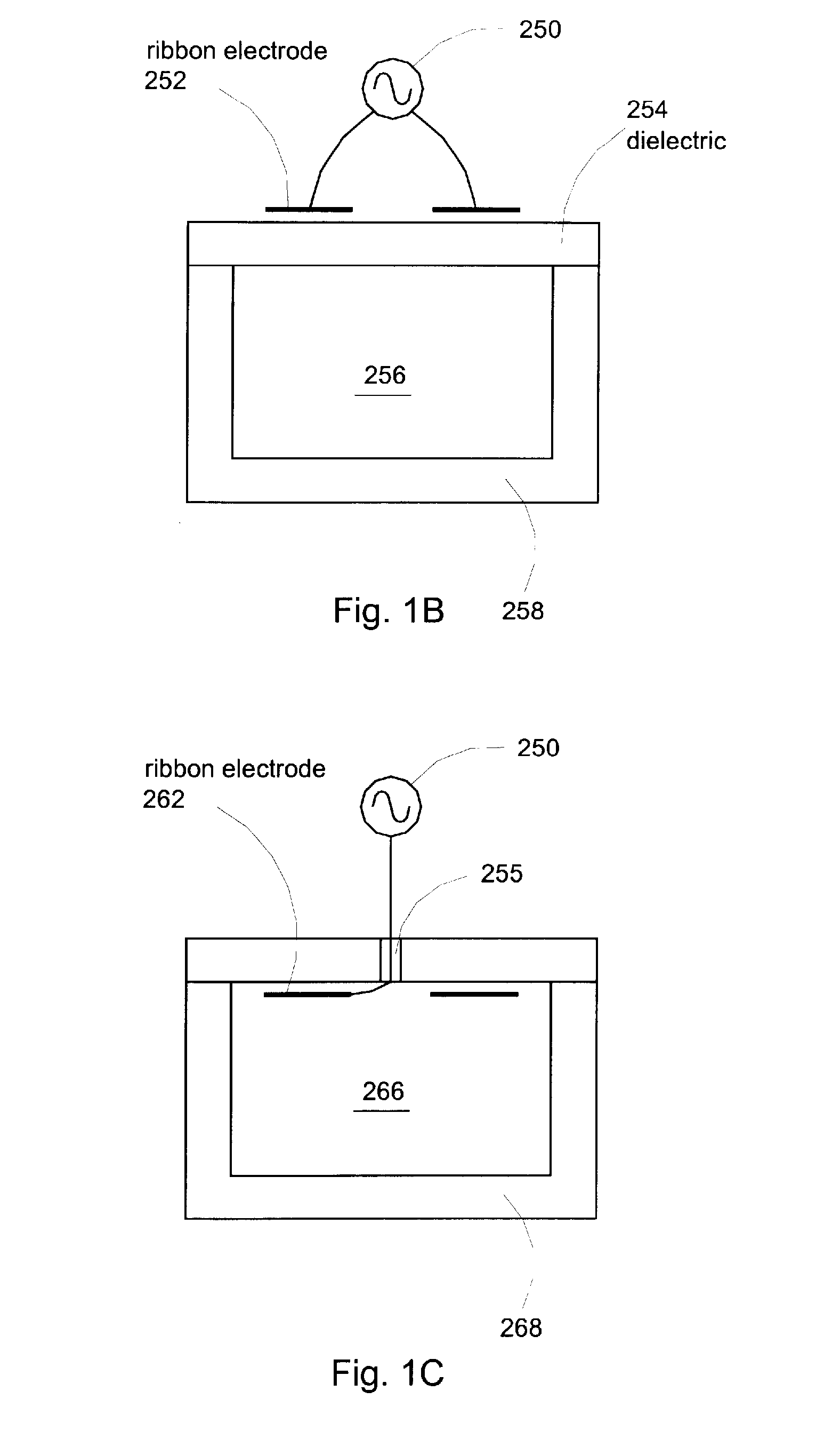
[0036]Turning now to FIG. 1B, a second embodiment is shown. FIG. 1B includes a helical ribbon electrode 252 connected to a generator 250. The helical ribbon electrode 252 rests above a dielectric wall 254. The dielectric wall 254 rests above a chamber 256 and is supported by chamber walls 258. The dielectric wall 254 allows the energy generated from the generator 250 to pass through to generate a plasma inside the chamber 256. The dielectric materials can be any non-metallic materials such as ceramics, glass, quartz, or plastic.
third embodiment
[0037]FIG. 1C shows a third embodiment where the helical ribbon electrode 262 is positioned inside a chamber 266 with walls 268. The walls 268 has a electrical feed through 255 through which the generator 250 can drive the helical ribbon electrode 262.
fourth embodiment
[0038]FIG. 1D shows a fourth embodiment where the helical ribbon electrode 272 wraps around a tubular dielectric wall 278. A chamber 276 is positioned within the helical ribbon electrode 272 and the tubular dielectric wall 278.
PUM
Property
Measurement
Unit
Thickness
aaaaa
aaaaa
Pressure
aaaaa
aaaaa
Thickness
aaaaa
aaaaa
Abstract
A process to deposit a thin film by chemical vapor deposition includes evacuating a chamber of gases; exposing a device to a gaseous first reactant, wherein the first reactant deposits on the device to form the thin film having a plurality of monolayers in thickness; evacuating the chamber of gases; exposing the device, coated with the first reactant, to a gaseous second reactant under a plasma treatment, wherein the thin film is treated by the first reactant; and repeating the previous steps.
Description
CROSS-REFERENCE TO RELATED APPLICATIONS[0001]This application is a continuation of U.S. application Ser. No. 12 / 783,431, filed May 19, 2010, entitled: “NANOLAYER DEPOSITION USING BIAS POWER TREATMENT”, which is a Continuation-In-Part Patent Application of U.S. application Ser. No. 11 / 739,637 filed Apr. 24, 2007, entitled: “NANOLAYER THICK FILM PROCESSING SYSTEM”, which is a Divisional Patent Application of U.S. application Ser. No. 10 / 790,652 filed Mar. 1, 2004, now U.S. Pat. No. 7,235,484, issued Jun. 26, 2007, entitled: “NANOLAYER THICK FILM PROCESSING SYSTEM AND METHOD”, which is a Continuation of application Ser. No. 09 / 954,244 filed on Sep. 10, 2001, now U.S. Pat. No. 6,756,318, issued Jun. 29, 2004, entitled: “NANOLAYER THICK FILM PROCESSING SYSTEM AND METHOD”, all of which are incorporated herein by reference.BACKGROUND OF THE INVENTION[0002]The present invention relates to semiconductor thin film processing. The fabrication of modern semiconductor device structures has tradi...
Claims
Application Information
Patent Timeline
Application Date:The date an application was filed.
Publication Date:The date a patent or application was officially published.
First Publication Date:The earliest publication date of a patent with the same application number.
Issue Date:Publication date of the patent grant document.
PCT Entry Date:The Entry date of PCT National Phase.
Estimated Expiry Date:The statutory expiry date of a patent right according to the Patent Law, and it is the longest term of protection that the patent right can achieve without the termination of the patent right due to other reasons(Term extension factor has been taken into account ).
Invalid Date:Actual expiry date is based on effective date or publication date of legal transaction data of invalid patent.
IPC IPC(8): H01L21/30
CPCC23C16/34C23C16/507C23C16/45523
Inventor DITIZIO, ROBERT ANTHONYNGUYEN, TUENGUYEN, TAI DUNG