Body contact structure for a semiconductor device
- Summary
- Abstract
- Description
- Claims
- Application Information
AI Technical Summary
Benefits of technology
Problems solved by technology
Method used
Image

Examples
example
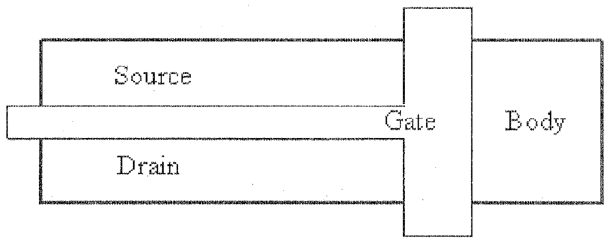
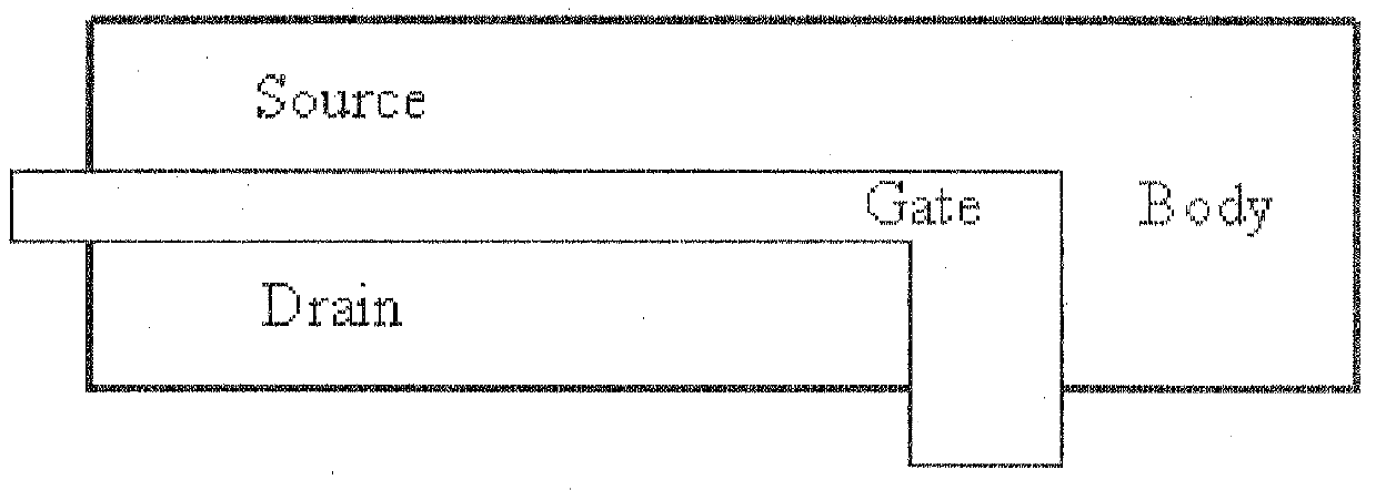
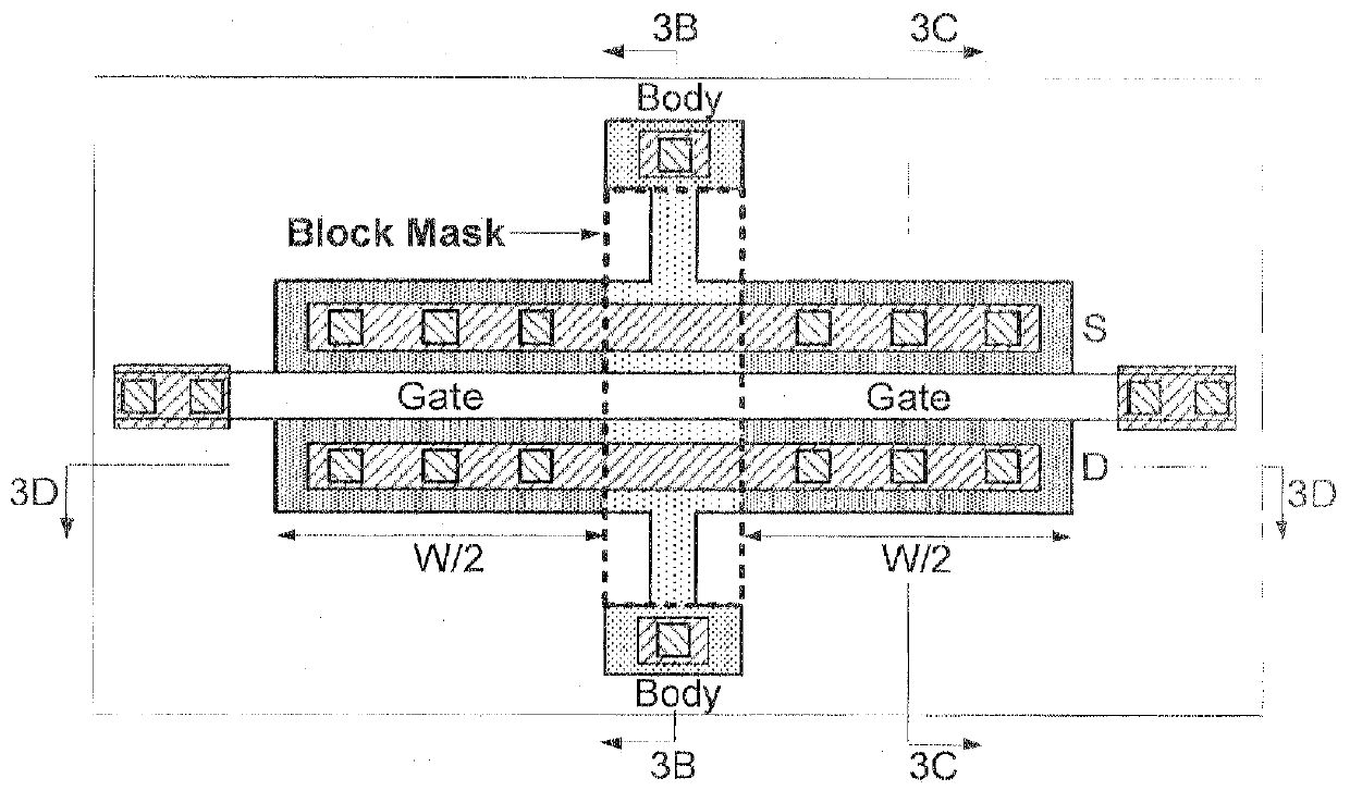
[0051]An I-gate BT SOI transistor according to an embodiment of the invention is fabricated, and exhibits comparable fT and fmax as that of a FB SOI transistor and comparable analog performance as that of a T-gate BT transistor. For the example embodiment, an I-Gate BT n-type transistor was designed according to the configuration shown in FIGS. 3A-3D.
[0052]For the example, embodiment, the n+ doped regions form drain and source, and the body region under the straight polysilicon line is p− doped. At the center of transistor / gate polysilicon, the source / drain implantation is blocked to form a p− region (0.2 μm wide) which is extended in the direction perpendicular to the width of the polysilicon gate. At the ends of extension, p+ body contacts are formed. A silicide block mask is used in the same source / drain implant blocked area (but not covering the body contact region) so that the extended body is not short circuited to a source or a drain through the silicide layer.
[0053]The split...
PUM
 Abstract
Description
Claims
Application Information
 - R&D
- Intellectual Property
- Life Sciences
- Materials
- Tech Scout
- Unparalleled Data Quality
- Higher Quality Content
- 60% Fewer Hallucinations
Browse by: Latest US Patents, China's latest patents, Technical Efficacy Thesaurus, Application Domain, Technology Topic, Popular Technical Reports.
© 2025 PatSnap. All rights reserved.Legal|Privacy policy|Modern Slavery Act Transparency Statement|Sitemap|About US| Contact US: help@patsnap.com