

Structure and method of making graphene nanoribbons
a graphene nanoribbon and graphene ribbon technology, applied in the direction of electrical/magnetic/electromagnetic heating, weaving, transportation and packaging, etc., can solve the problems of unreliable gnr property, art does not disclose the cnt diameter control necessary, and both methods of creating sub-10 nm wide graphene nanoribbons have manufacturability problems, etc., to achieve the effect of increasing the number of intermolecular bonds
- Summary
- Abstract
- Description
- Claims
- Application Information
AI Technical Summary
Benefits of technology
Problems solved by technology
Method used
Image

Examples
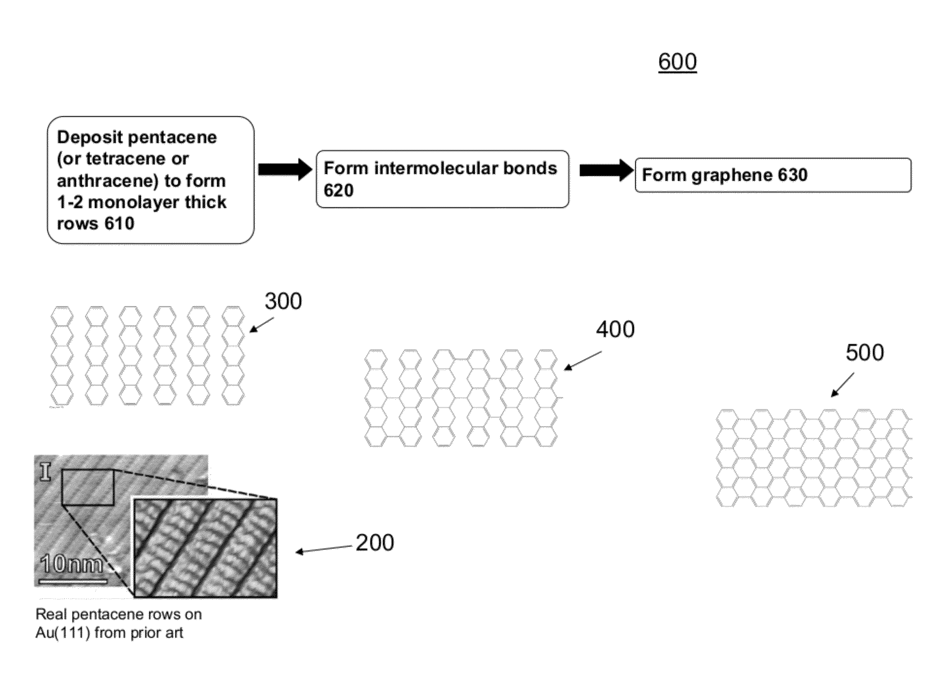
embodiment 1
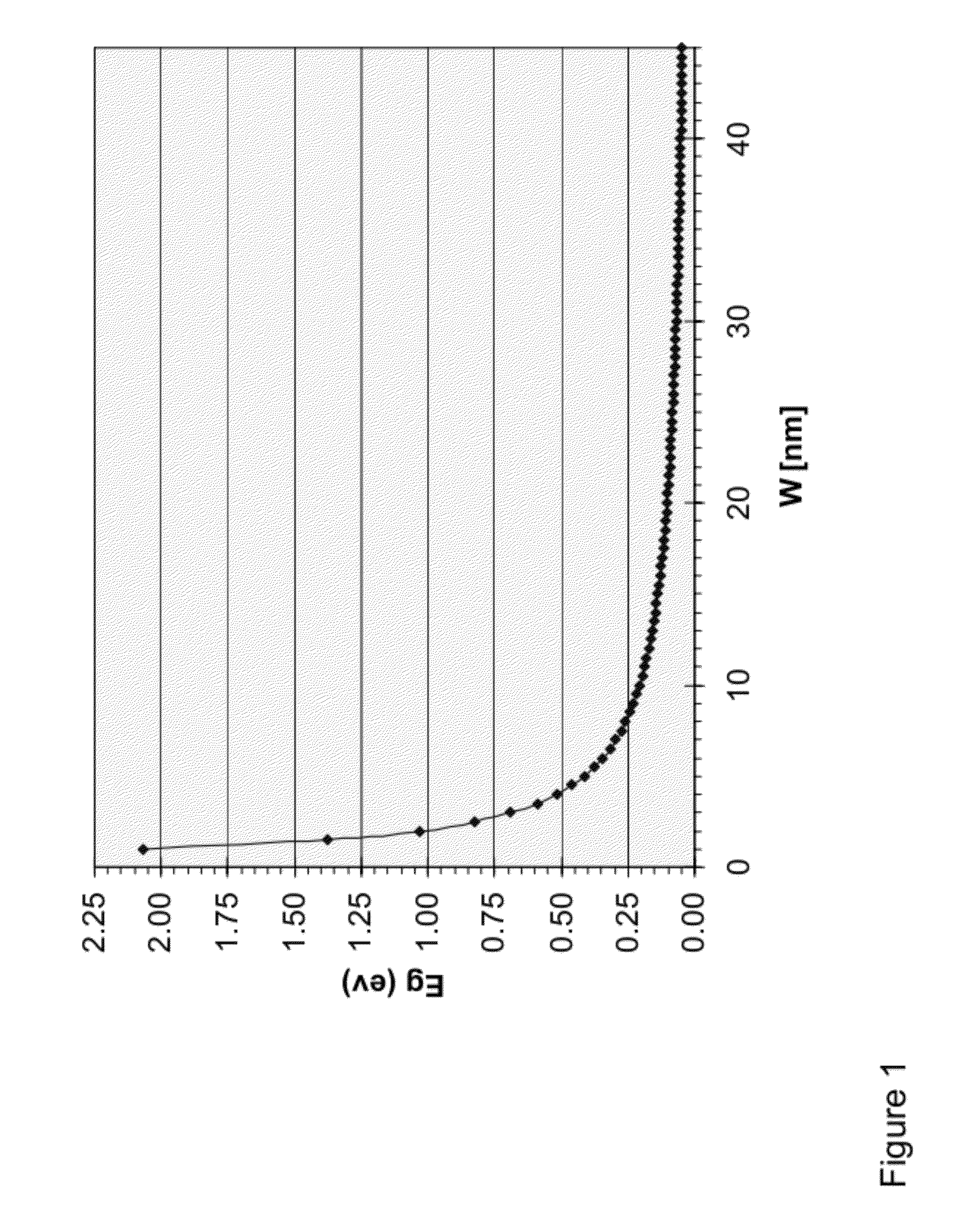
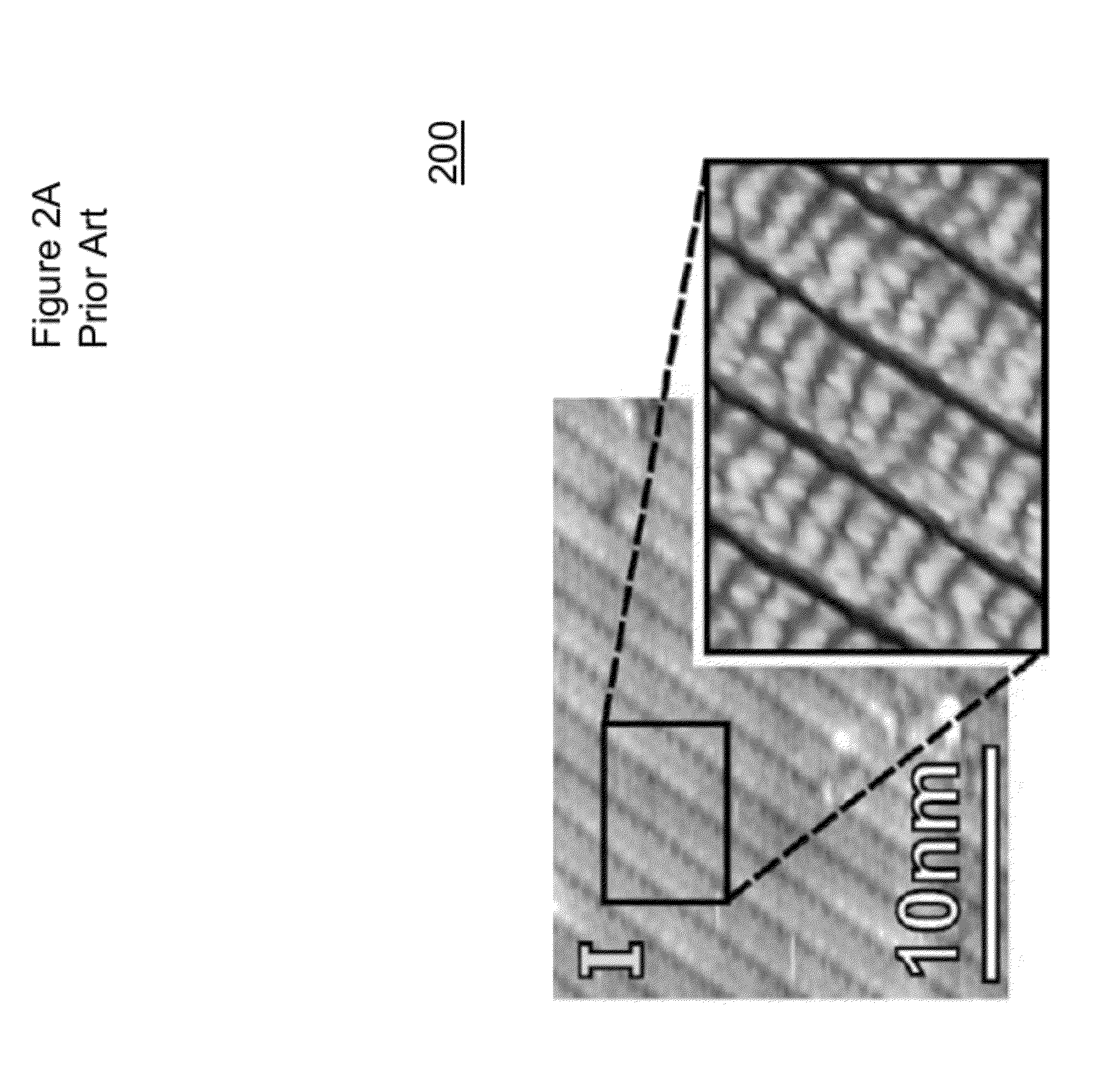
[0094]Pentacene molecules, which have a length just above 1.5 nm, can grow parallel ribbons of the same width separated by a narrow gap from a nearest neighbor (nn) ribbon on appropriate surfaces. The pentacene molecules lie with their long axis practically parallel to the surface and practically perpendicular to the direction of the strip, as shown in FIG. 1 below taken from [Käfer D. et al. Phys.Rev. B 75, 085309 (2007)]. This specific figure shows pentacene molecules self-assembled on a Au (111) surface, but other judiciously chosen surfaces could also be used to grow similar pentacene structures, preferably insulating surfaces or surfaces that could be removed later, at the device fabrication stage. Deposition of pentacene molecules can take place using a molecular beam deposition method similar to the one described in the art (Dimitrakopoulos et al. J. Appl. Phys. J. of Appl. Phys., 80, 2501-2508, (1996) “Molecular beam deposited thin films of pentacene for organic field effect...
embodiment 2
[0101]The method of embodiment 1 can be used with one difference: The pentacene molecule is replaced by tetracene, an acene molecule with four fused aromatic rings instead of the five fused aromatic rings of pentacene (FIG. 7). This will result to even shorter GNRs (thus with even wider band gap) than pentacene.
embodiment 3
[0102]The method of embodiment 1 can be used with one difference: The pentacene molecule is replaced by anthracene, an acene molecule with three fused aromatic rings instead of the five fused aromatic rings of pentacene. This will result to even shorter GNRs (thus with even wider band gap) than tetracene.
PUM
| Property | Measurement | Unit |
|---|---|---|
| thickness | aaaaa | aaaaa |
| thickness | aaaaa | aaaaa |
| width | aaaaa | aaaaa |
Abstract
Description
Claims
Application Information