Light-Emitting Device and Manufacturing Method Thereof

Active Publication Date: 2012-11-01
SEMICON ENERGY LAB CO LTD
View PDF13 Cites 33 Cited by
  • Summary
  • Abstract
  • Description
  • Claims
  • Application Information

AI Technical Summary

Benefits of technology

[0031]A black matrix, a light-blocking spacer, and a partition overlap with one another, whereby a panel structure in which a space between a pair of substrates can be kept uniform can be provided when the space between the pair of sub

Problems solved by technology

However, in this structure, there is a problem in that an aperture ratio is limited because o

Method used


Image

  • Light-Emitting Device and Manufacturing Method Thereof
  • Light-Emitting Device and Manufacturing Method Thereof
  • Light-Emitting Device and Manufacturing Method Thereof

Examples


Example

Embodiment 1

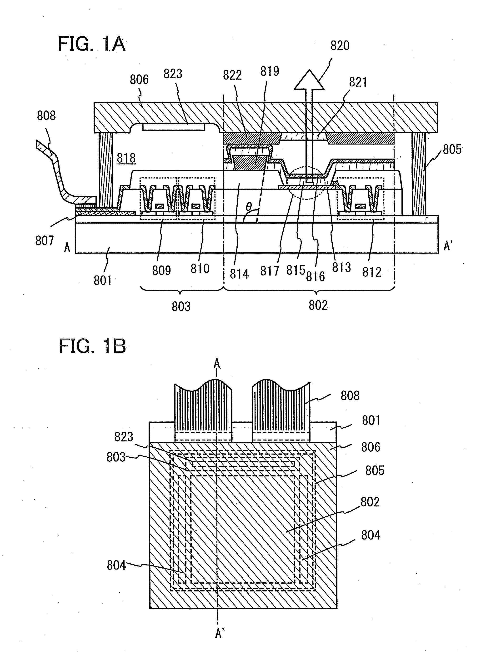
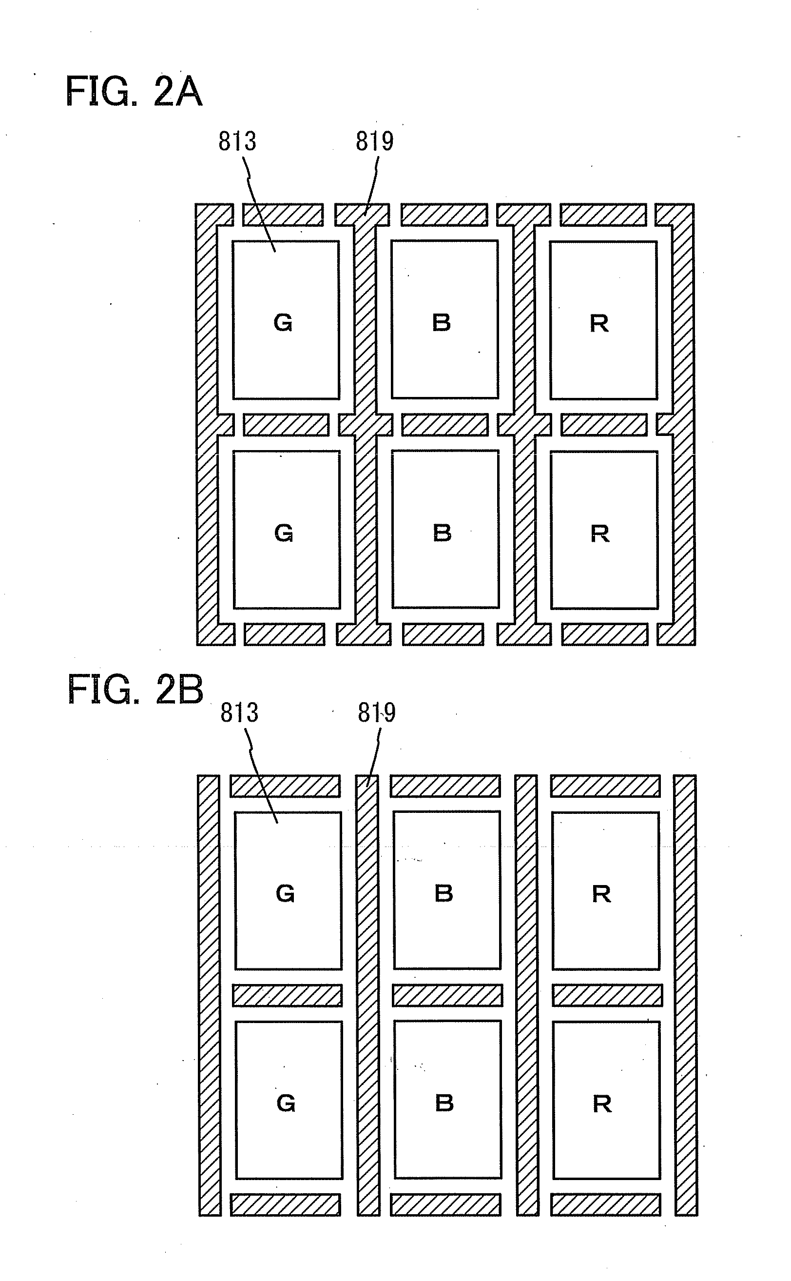
[0040]An example of an active matrix light-emitting device will be described with reference to FIGS. 1A and 1B. Note that FIG. 1B is a plan view of a light-emitting device and FIG. 1A is a cross-sectional view taken along dashed line A-A′ in FIG. 1B.

[0041]The active matrix light-emitting device of this embodiment includes a pixel portion 802 provided over a glass substrate 801, a driver circuit portion (a source line driver circuit) 803, and a driver circuit portion (a gate line driver circuit) 804. The pixel portion 802, the driver circuit portion 803, and the driver circuit portion 804 are sealed in a space surrounded by a fixing portion 805, the glass substrate 801, and a glass substrate 806. In the glass substrate 806, a depression portion (also referred to as a drilled hole) is formed in a region other than a region overlapping with the pixel portion 802, and a desiccant 823 is provided for the depression portion for ensuring reliability of the light-emitting elemen...

Example

Embodiment 2

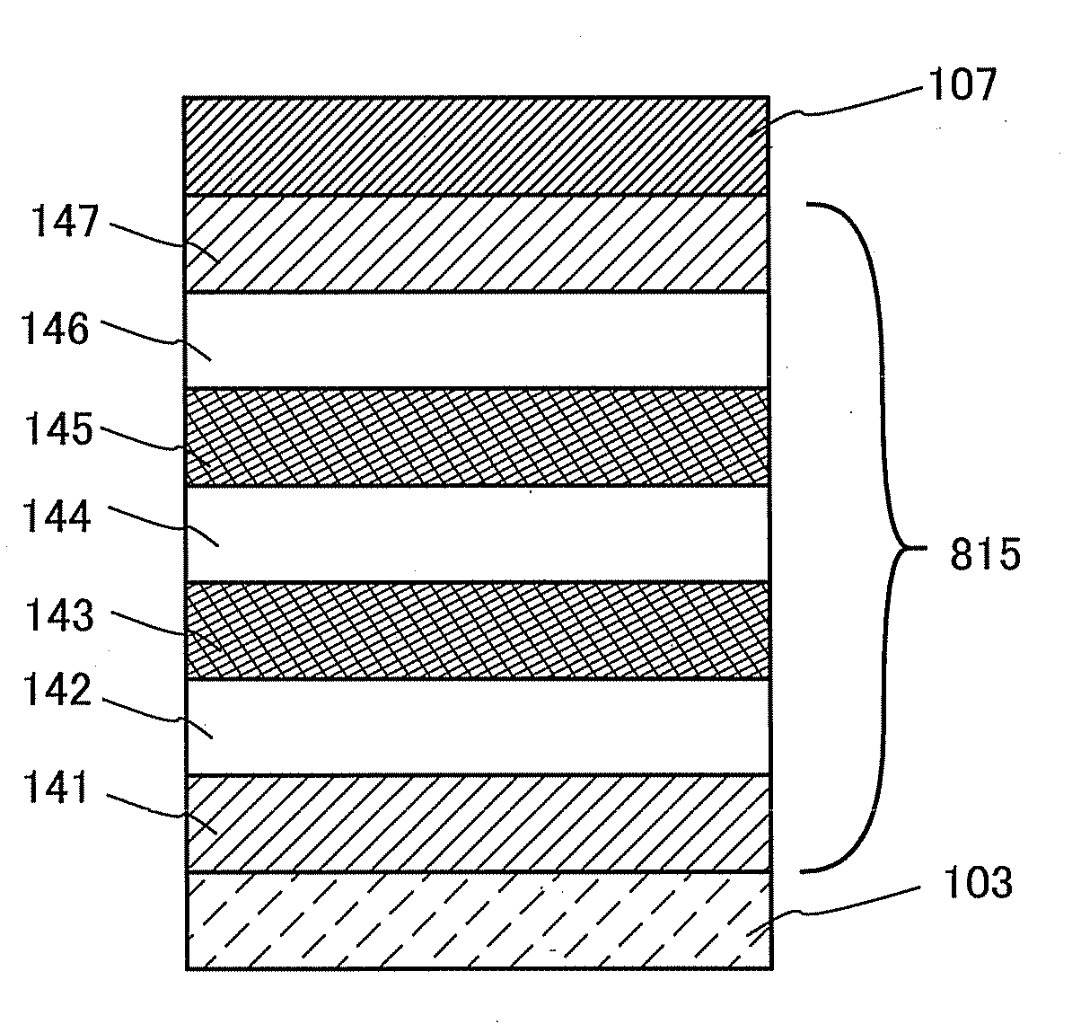
[0058]In this embodiment, a specific example of a stack of the layer 815 containing an organic compound described in Embodiment 1 will be described with reference to FIG. 4.

[0059]Over a first electrode layer 103, a hole-injection layer 141, a first light-emitting unit 142, an intermediate layer 143, a second light-emitting unit 144, an intermediate layer 145, a third light-emitting unit 146, an electron-injection layer 147, and a second electrode layer 107 are stacked in this order. For the first electrode layer 103, an element belonging to Group 1 or 2 of the periodic table, that is, an alkali metal such as lithium (Li) or cesium (Cs), an alkaline earth metal such as calcium (Ca) or strontium (Sr), or magnesium (Mg) can be used. Further, an alloy containing an alkali metal, an alkaline earth metal, or magnesium (e.g., MgAg or AlLi) can be used. Moreover, a rare earth metal such as europium (Eu) or ytterbium (Yb), or an alloy containing a rare earth metal can also be use...

Example

Embodiment 3

[0075]In this embodiment, specific examples of electronic devices each of which is manufactured using the light-emitting device described in the above embodiments will be described with reference to FIGS. 6A to 6D.

[0076]Examples of electronic devices to which the present invention can be applied include a television set (also referred to as a television or a television receiver), a monitor of a computer or the like, a digital camera, a digital video camera, a digital photo frame, a mobile phone, a portable game machine, a portable information terminal, an audio reproducing device, a game machine (e.g., a pachinko machine or a slot machine), a housing of a game machine, and the like. Specific examples of these electronic devices are shown in FIGS. 6A to 6D.

[0077]FIG. 6A illustrates a table9000 having a display portion. In the table 9000, a display portion 9003 is incorporated into a housing 9001. A light-emitting device manufactured according to an embodiment of the prese...


PUM


Abstract

When a hollow structure in which a light-emitting element is provided between a pair of substrates is used in order to prevent oxygen or moisture from reaching the light-emitting element, light leakage to an adjacent pixel easily occurs as compared to a structure in which a space between a pair of substrates is filled with a resin such as an adhesive. In order to reduce light leakage to an adjacent pixel in the hollow structure, a light-blocking spacer is formed over a partition to keep the distance between the pair of substrates uniform. The cross-sectional shape of the light-blocking spacer is a trapezoid having a lower side shorter than an upper side.

Description

BACKGROUND OF THE INVENTION[0001]1. Field of the Invention[0002]The present invention relates to a light-emitting device in which a layer including an organic compound serves as a light-emitting layer and a method for manufacturing the light-emitting device.[0003]2. Description of the Related Art[0004]A light-emitting element containing an organic compound as a luminous body, which has features such as thinness, lightness, high-speed response, and DC drive at a low voltage, is expected to be applied to a next-generation flat panel display or a next-generation lighting device.[0005]A light-emitting mechanism of a light-emitting element is as follows: a voltage is applied between a pair of electrodes where a layer containing an organic compound is interposed, electrons injected from a cathode and holes injected from an anode are recombined with each other at an emitting center of the layer containing an organic compound (also referred to as an EL layer) to form molecular excitons, and...

Claims


Application Information

Patent Timeline
IPC IPC(8): H01L33/00
CPCH01L51/525Y02E10/549H10K50/8428H10K77/10H10K50/865H01L27/1214H10K59/126H10K50/844H10K59/35H10K59/124H10K59/125H10K59/127H10K59/1213
Inventor HATANO, KAORU
Owner SEMICON ENERGY LAB CO LTD
Why Eureka
Try Eureka