Group iii nitride semiconductor laser device, epitaxial substrate, method of fabricating group iii nitride semiconductor laser device

a laser device and semiconductor technology, applied in semiconductor devices, lasers, semiconductor lasers, etc., can solve the problems of reducing the critical thickness, reducing the thickness of the algan cladding layer, and increasing the aluminum content of the algan, so as to reduce the strain and reduce the effective refractive index

Inactive Publication Date: 2012-12-27
SUMITOMO ELECTRIC IND LTD +1
View PDF3 Cites 15 Cited by
  • Summary
  • Abstract
  • Description
  • Claims
  • Application Information

AI Technical Summary

Benefits of technology

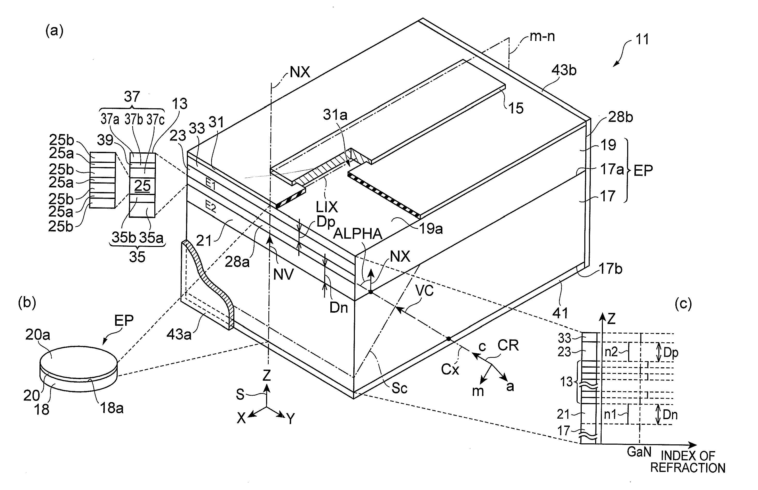
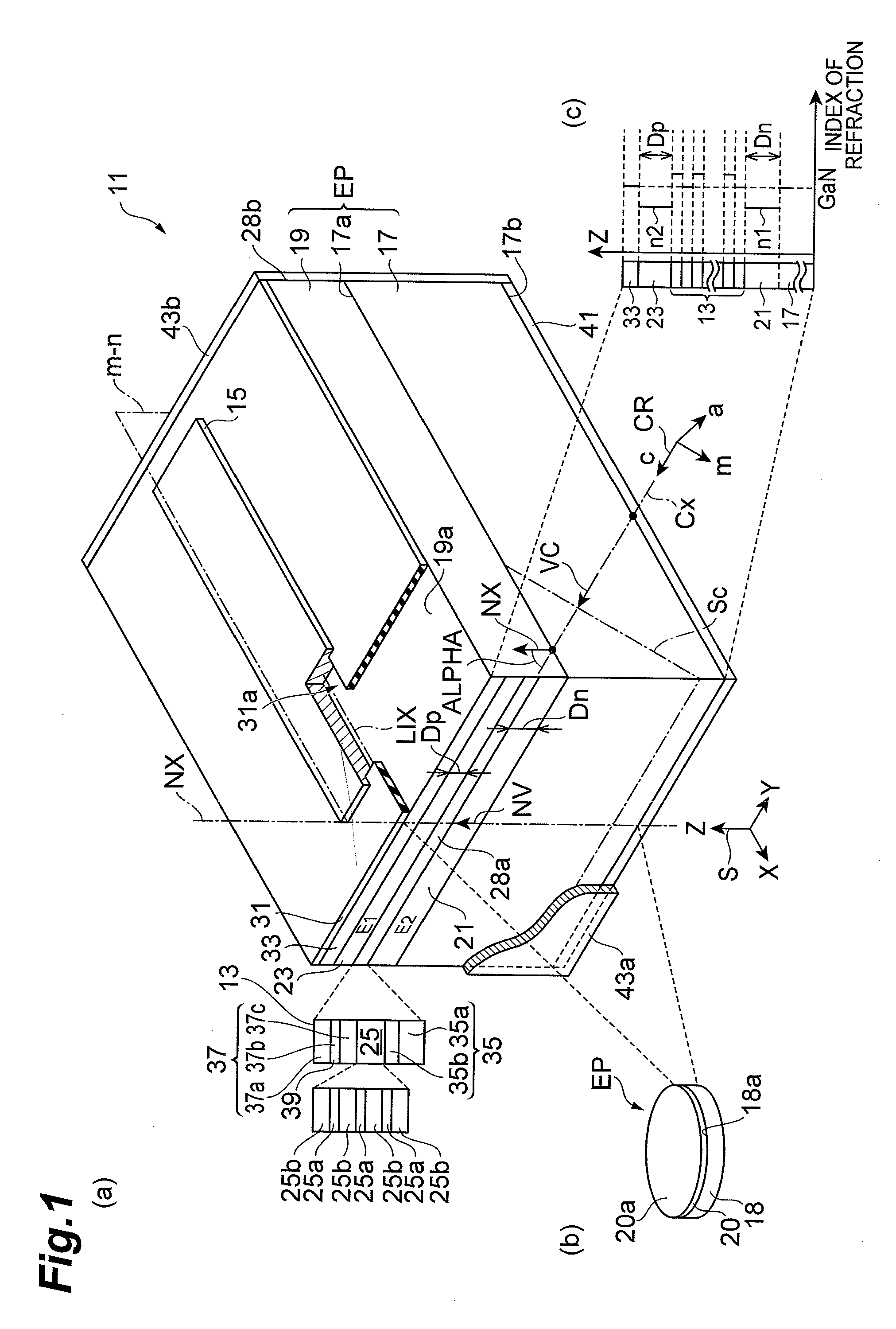
[0039]The optical guiding regions provided between the active layer and the respective cladding layers include at least two layers (InGaN layer and GaN layer) each having a refraction index different from one another, thereby reducing strain and avoid a decrease in the difference between the refractive index of the cladding and the refractive index of the core.
[0040]The nitride semiconductor laser device and the epitaxial substrate according to the above aspects of the present invention may further includ

Problems solved by technology

The thickness of such an AlGaN cladding layer is also limited by the critical thickness.
But, the thickness of an AlGaN cladding layer is limited by the critical thickness whereas an increase in the aluminum content in the AlGaN reduces the critical thickness.
Changing the thickness of the cladding layer is not enough

Method used


Image

  • Group iii nitride semiconductor laser device, epitaxial substrate, method of fabricating group iii nitride semiconductor laser device
  • Group iii nitride semiconductor laser device, epitaxial substrate, method of fabricating group iii nitride semiconductor laser device
  • Group iii nitride semiconductor laser device, epitaxial substrate, method of fabricating group iii nitride semiconductor laser device

Examples


example 1

[0132]FIG. 8 is a schematic view showing a group-III nitride semiconductor laser device according to Example 1. Part (a) of FIG. 8 is a schematic view showing the structure of the group-III nitride semiconductor laser device. Such a group-III nitride semiconductor laser device is produced under the process conditions listed in part (b) of FIG. 8.

[0133]A group-III nitride substrate is prepared which has a semi-polar front surface. In this example, a GaN substrate 51 which is prepared has a semi-polar front surface tilting toward the m-axis at an angle of 75 degrees. The plane orientation of the semi-polar front surface corresponds to the {20-21} plane. A semiconductor region having an LD structure LD1 operable in a lasing wavelength band of 520 nm is grown on the semi-polar front surface of the GaN substrate 51. The GaN substrate 51 is placed in a growth reactor for pre-processing (thermal cleaning). Such pre-processing is performed in an ammonia and hydrogen atmosphere for ten minut...

example 2

[0140]FIG. 10 is a drawing illustrating the structure of a semiconductor laser device composed of an epitaxial substrate having several laser structures formed on the (20-21) GaN plane. Several laser epitaxial structures are grown on the (20-21) GaN plane under growth conditions that are the same as those in Example 1 except for the thickness of the cladding layer. The laser epitaxial structure illustrated in part (a) of FIG. 10 is the same as the structure in Example 1. Referring to part (b) of FIG. 10, the n-type cladding layer has a large thickness. Referring to part (c) of FIG. 10, the n-type and p-type cladding layers have a large thickness.

[0141]An epitaxial substrate having such a laser epitaxial structure is made through a laser production process, such as that described below. An insulating layer, such as a silicon dioxide layer, is grown on the laser epitaxial structure. Then, wet-etching is applied to the insulating layer in order to form a window of a strip shape with a ...


PUM


Abstract

A nitride semiconductor laser device includes a p-type cladding layer, an active layer and an n-type cladding layer. The p-type cladding layer and the n-type cladding layer comprise indium and aluminum as group-III constituent. The n-type cladding layer, active layer and p-type cladding layer are arranged along the normal of a semi-polar semiconductor surface of a substrate. This surface tilts toward the m-axis of the hexagonal nitride by an angle of 63 degrees or more and smaller than 80 degrees from a plane orthogonal to a reference axis extending along the c-axis thereof. The active layer generates light having a peak wavelength in the range of 480 to 600 nm. The refractive indices of the n-type cladding layer and p-type cladding layer are smaller than that of GaN. The n-type cladding layer has a thickness of 2 μm or more while the p-type cladding layer has a thickness of 500 nm or more.

Description

BACKGROUND OF THE INVENTION[0001]1. Field of the Invention[0002]The present invention relates to a nitride semiconductor laser device, an epitaxial substrate, and a method of fabricating a nitride semiconductor laser device.[0003]2. Related Background Art[0004]Patent Literature 1 discloses a nitride semiconductor light-emitting device formed on a c-plane. The nitride semiconductor light-emitting device includes two ternary AlGaN cladding layers. The light emitted from the nitride semiconductor light-emitting device has a wavelength between approximately 410 and 455 nm, which is a wavelength equal to or shorter than that of blue light.[0005]Patent Literature 1: Japanese Patent No. 3538275SUMMARY OF THE INVENTION[0006]As mentioned in Patent Literature 1, a thick AlGaN cladding layer cracks. The thickness of such an AlGaN cladding layer is also limited by the critical thickness.[0007]The light emitting device disclosed in Patent Literature 1 emits light having a wavelength in the range...

Claims


Application Information

Patent Timeline
IPC IPC(8): H01S5/323H01L33/32
CPCH01L21/02389B82Y20/00H01L21/02458H01L21/0254H01L21/0262H01S5/0202H01S5/028H01S5/0425H01S5/2009H01S5/2031H01S5/3201H01S5/3202H01S5/3211H01S5/34333H01S2301/176H01S2304/04H01L21/02433H01S5/320275
Inventor ENYA, YOHEIYOSHIZUMI, YUSUKEKYONO, TAKASHISUMITOMO, TAKAMICHIUENO, MASAKIYANASHIMA, KATSUNORITASAI, KUNIHIKONAKAJIMA, HIROSHI
Owner SUMITOMO ELECTRIC IND LTD
Why Eureka
Try Eureka