

Article with metal grid composite and methods of preparing
a technology of metal grid and composite, applied in the direction of conductive layers on insulating supports, transportation and packaging, chemistry apparatus and processes, etc., can solve the problems of cumbersome methods using lithographic techniques, high cost of articles, and laborious and costly materials and manufacture, and achieve improved planarity and uniform conductivity. , the effect of improving the topography
- Summary
- Abstract
- Description
- Claims
- Application Information
AI Technical Summary
Benefits of technology
Problems solved by technology
Method used
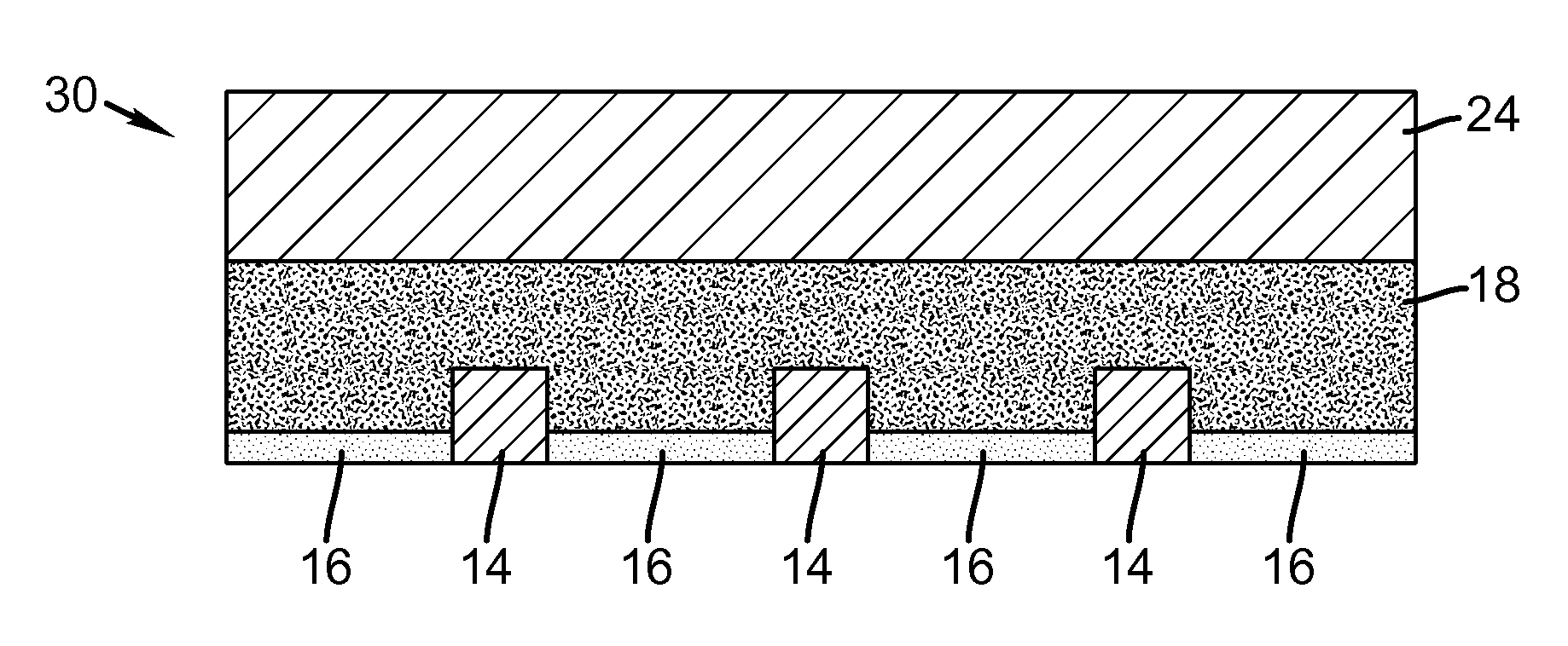
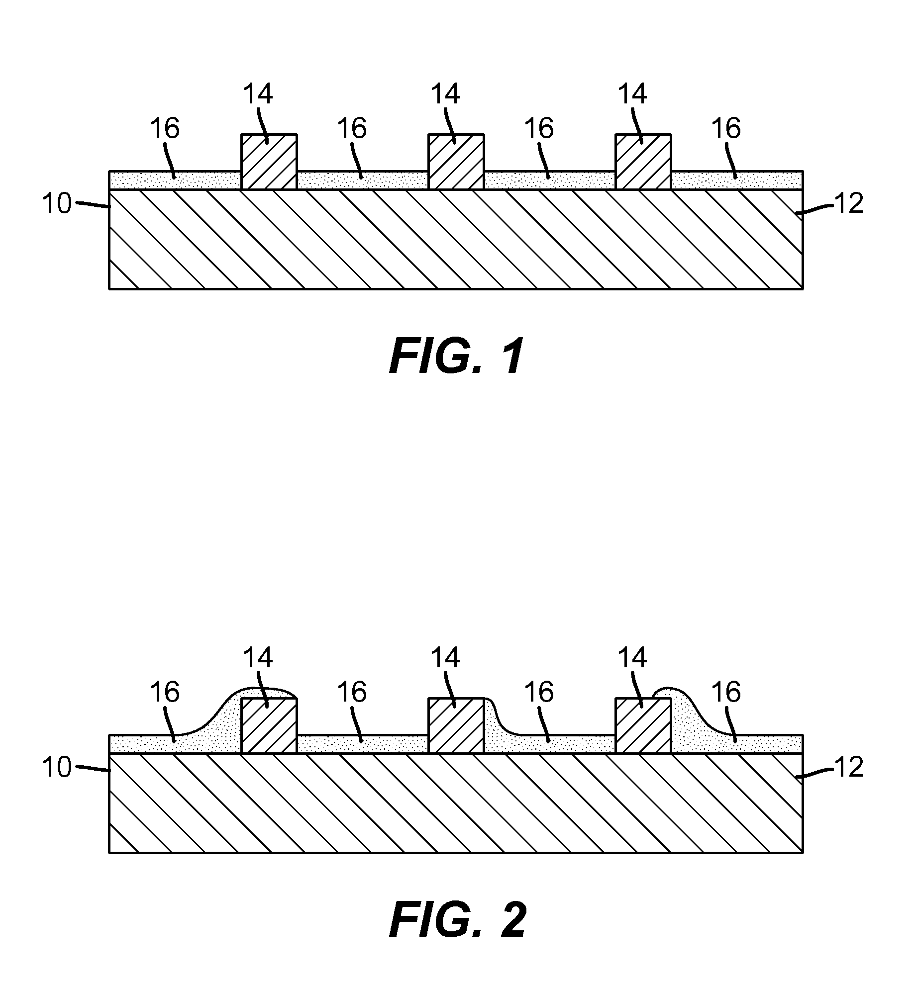
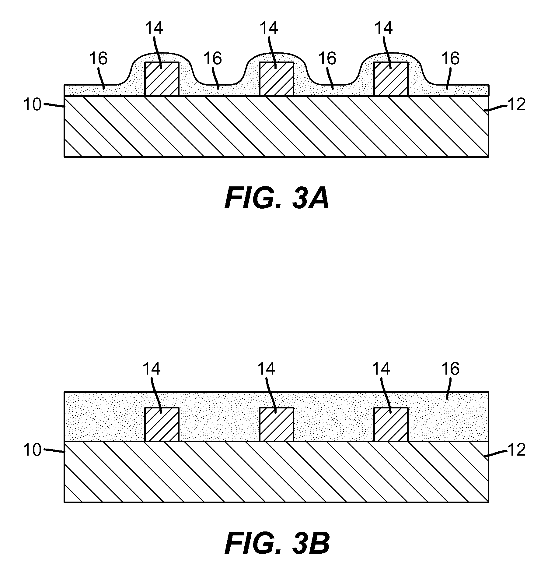
Image

Examples
invention example 1
[0196]A laminate donor element of this invention was prepared in the following manner:
[0197]A donor substrate was chosen as a 100 micrometer thick uncoated poly(ethylene terephthalate) (PET) film. This donor substrate was treated on one side with corona discharge and flexographically printed with a metal grid having a random pattern of interconnected silver lines using a commercially available nanoparticulate silver ink dispersion (such as one obtained from PChem Associates). This metal grid of silver lines was further coated with the following Formulation A containing an electronically conductive polymer to provide a wet coverage of 32 cm3 / m2. Upon drying, the electronically conductive polymer was located in the voids among the silver lines and directly on the donor substrate.
Formulation A
[0198]
Formulation AIngredientsDescription of ingredientsWeight %Clevios ™ PH 1000PEDOT: PSS* dispersion (1.384.9(as received)weight % in water) supplied byHeraeusSilquest ® Aγ-Glycidoxypropyltrime...
PUM
| Property | Measurement | Unit |
|---|---|---|
| Length | aaaaa | aaaaa |
| Length | aaaaa | aaaaa |
| Length | aaaaa | aaaaa |
Abstract
Description
Claims
Application Information