Photodetector device with protective and antireflective cover, and manufacturing method thereof

a technology of photodetector and protective cover, which is applied in the direction of photometry, photometry using electric radiation detector, instruments, etc., can solve the problems of low quantum efficiency of these devices in the range of uv wavelengths, limited or at times disadvantageous use, and large dimensions

Active Publication Date: 2013-01-24
STMICROELECTRONICS SRL
View PDF11 Cites 47 Cited by
  • Summary
  • Abstract
  • Description
  • Claims
  • Application Information

AI Technical Summary

Benefits of technology

[0023]According to the present approach a photodetector device with a cover layer of an improved type and a corresponding manufacturing method are provided. The present embodiments are directed to a photodetector device including a semiconductor body, having a front surface, and an active-area region which extends in the semiconductor body facing the front surface, configured for receiving a light radiation and generating, by the photoelectric effect in response to the light radiation received, electrical-charge carriers (in particular, an electron-hole pair, which, under the effect of an electrical field, generates an electric current). The photodetector device further includes a polydimethylsiloxane (PDMS) cover layer, which extends on the front surface in the active-area region so that the light radiation is received by the active-area region through the cover layer. The cover layer offers protection for the front surface of the semiconductor body and acts as antireflective layer for the light radiation received. The light radiation is, in particular, a UV radiation.

Problems solved by technology

However, known photomultiplier tubes present some disadvantages that render use thereof limited or at times disadvantageous.
For example, the quantum efficiency of these devices in the range of the UV wavelengths is low, they have large dimensions, high costs, require high biasing voltages, and are fragile.
However, the sensitivity of these devices is usually low for wavelengths shorter than 300 nm, on account of the absorption of the ultraviolet radiation by the metal layer.
This approach, however, can cause a problematic control of the uniformity of thickness of the Schottky barrier (which is extremely thin), with consequent problems of poor thermal and mechanical stability.
Such process is relatively slow and can lead to a final layer containing crystallographic defects.
By introducing a small amount of hydrochloric acid (HCl) into the oxidation oven, or another gas containing chlorine (for example TCE—trichloroethylene), it is possible to reduce the number of crystallographic defects of the layer grown, but there is the disadvantage of obtaining an oxide layer containing a certain percentage of chlorine.
The PECVD and LPCVD techniques enable deposition of silicon oxide at lower temperatures, but the oxide layer that is obtained presents a poor structural quality, in particular from a stoichiometric standpoint and the standpoint of density.
Irrespective of the particular technique of deposition or growth adopted, further disadvantages of an antireflective layer of silicon oxide on silicon carbide involve high stresses on the SiC-SiO2 interface (in particular, for thick oxides), which can cause generation of leakage current and, in extreme cases, breakdown of the entire wafer.
The undesirable effect caused by the trapped charges is even more evident for low surface-doping levels, required when the device is operated at low reverse voltages.
Further disadvantages due to the presence of the protective SiO2 layer comprise a reduction of the response time of the photodetector, an increase of the dark current, and an increase of the leakage currents.
However, on account of the differences in the crystalline structure between silicon carbide and silicon nitride, and / or on account of defects in the crystallographic structure of the silicon-nitride layer, voltages can be set up in the silicon-nitride layer that may even cause breakdown thereof.
It is evident that the problems generated by the use of protective layers of silicon nitride or silicon oxide are not limited to photodetector devices with substrates made of silicon carbide, but extend to generic substrates of semiconductor material, such as, for example, silicon, gallium, gallium arsenide, gallium nitride, and others still.
Currently, packagings comprise a metal load-bearing structure provided with a ultraviolet-degree quartz window, which enables access of photons to the active area of the photodetector; however, the quartz window has a high cost.
Plastic packagings are used to reduce costs, but may not guarantee an optimal protection from impact, vibrations, and other external factors.
Furthermore, they may not form an adequate protective layer at high transmissivity in the ultraviolet, especially below 300 nm.

Method used


Image

  • Photodetector device with protective and antireflective cover, and manufacturing method thereof
  • Photodetector device with protective and antireflective cover, and manufacturing method thereof
  • Photodetector device with protective and antireflective cover, and manufacturing method thereof

Examples


Embodiment Construction

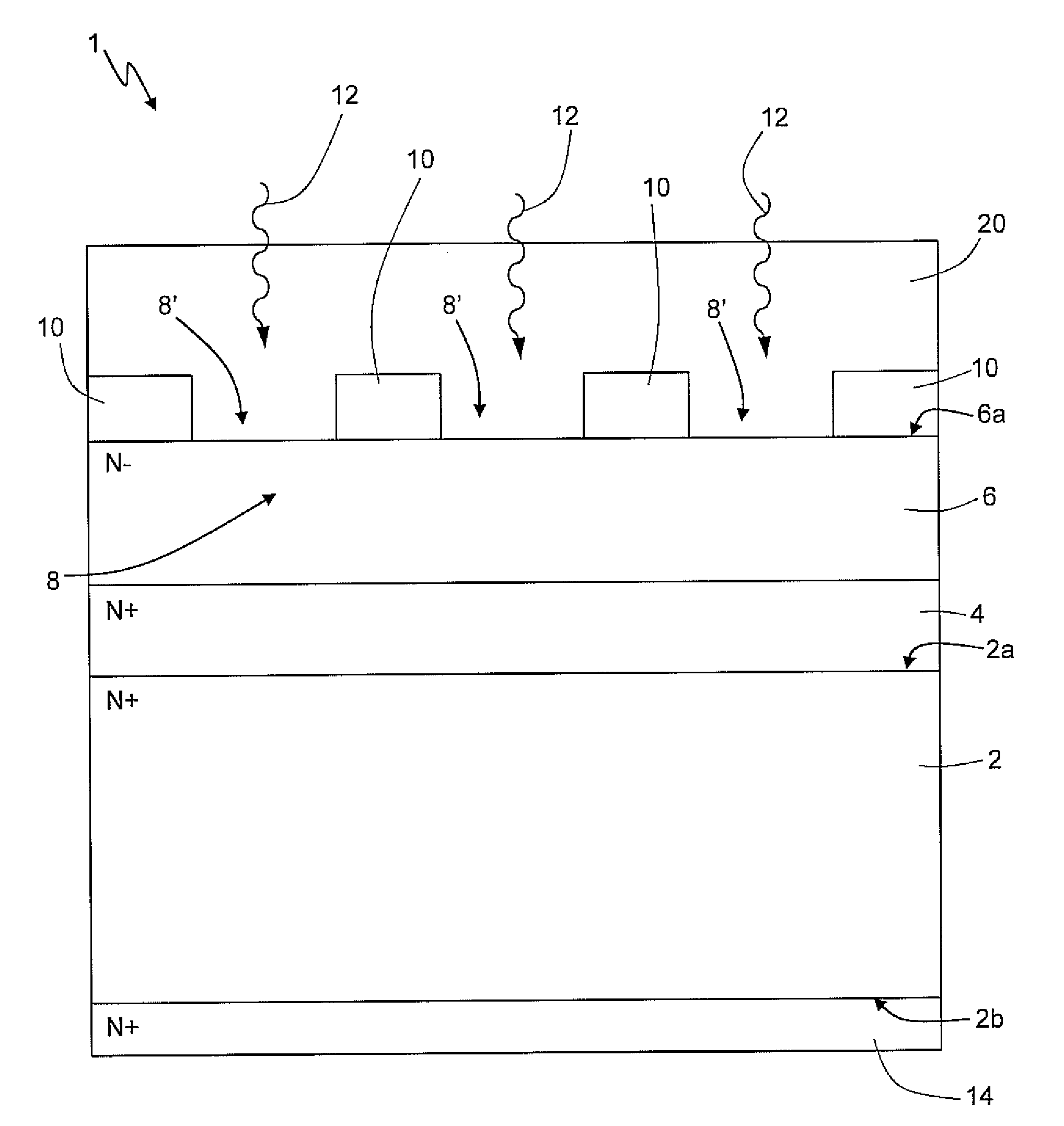
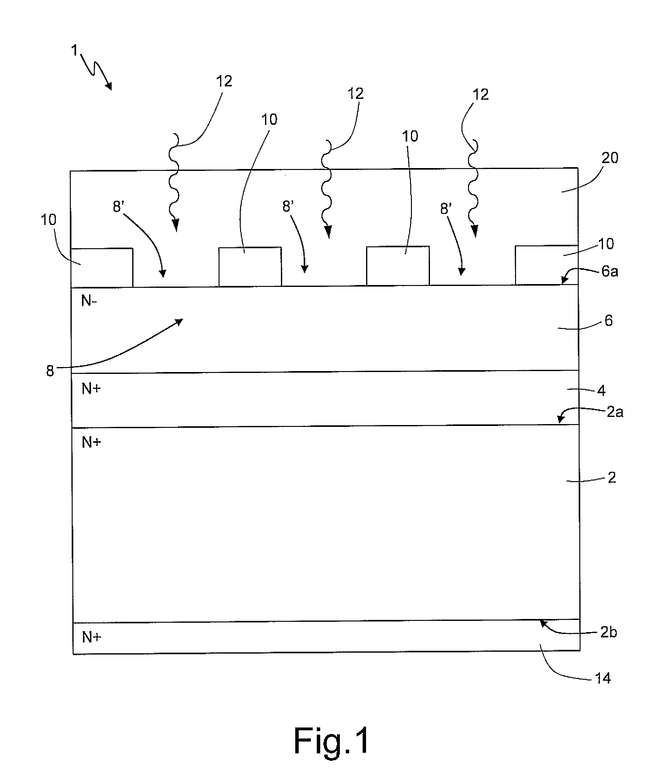
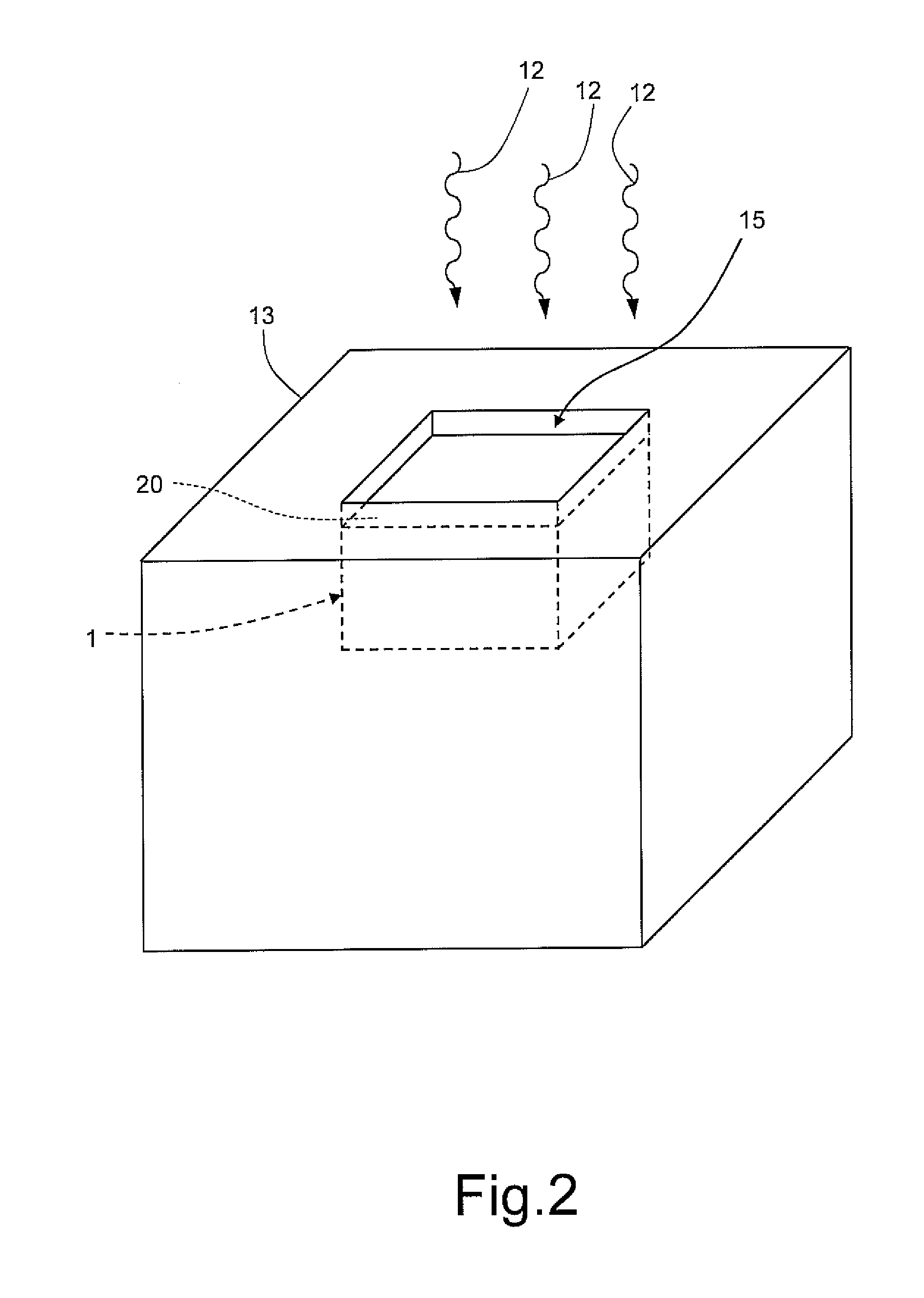
[0035]The present embodiments relate to a photodetector device including a semiconductor body, having a front surface, and an active-area region which extends in the semiconductor body facing the front surface, configured for receiving a light radiation and generating, by the photoelectric effect in response to the light radiation received, electrical-charge carriers (in particular, an electron-hole pair, which, under the effect of an electrical field, generates an electric current). The photodetector device further includes a polydimethylsiloxane (PDMS) cover layer, which extends on the front surface in the active-area region so that the light radiation is received by the active-area region through the cover layer. The cover layer offers protection for the front surface of the semiconductor body and acts as antireflective layer for the light radiation received. The light radiation is, in particular, a UV radiation. The particular physical structure of the photodetector device is ir...


PUM


Abstract

The photodetector device includes a semiconductor body having a front surface, and an active-area region that extends in the semiconductor body facing the front surface and is configured for receiving a light radiation and generating, in response to the light radiation received, electric charge carriers. A polydimethylsiloxane cover layer extends on the front surface in the active-area region so that the light radiation is received by the active-area region through the cover layer.

Description

FIELD OF THE INVENTION[0001]The present invention relates to a photodetector device provided with a cover layer designed to act as antireflective and protective layer, and to a corresponding manufacturing method.BACKGROUND OF THE INVENTION[0002]The wavelengths of ultraviolet (UV) radiation are between approximately 100 nm and approximately 400 nm, and, within this range, are divided into three bands: band A (UV-A), including wavelengths between approximately 315 nm and 400 nm; band B (UV-B), including wavelengths between approximately 280 and 315 nm; and band C (UV-C), including wavelengths between approximately 100 and 280 nm. Recently, the growth of applications in which ultraviolet radiation or signals are used has increased the interest in devices designed to detect wavelengths in the ultraviolet range, in particular devices having a high value of the signal-to-noise ratio. Such applications include, for example, detection of biological agents via induced fluorescence, steriliza...

Claims


Application Information

Patent Timeline
Patent Type & Authority Applications(United States)
IPC IPC(8): G01J1/44H01L31/18H01L31/0203
CPCH01L31/02161G01J1/429H01L31/1085H01L31/0312
Inventor MAZZILLO, MASSIMO CATALDO
Owner STMICROELECTRONICS SRL
Why Eureka
Try Eureka