Method of manufacturing single crystal 3c-sic substrate and single crystal 3c-sic substrate obtained from the manufacturing method

a manufacturing method and technology of applied in the field of manufacturing single crystal 3csic substrate obtained from the manufacturing method, can solve the problems of degradation of performance and quality of the gan layer, and achieve the effect of reducing surface pits, maintaining surface flatness, and high flatness

Active Publication Date: 2013-02-14
AIR WATER INC
View PDF2 Cites 9 Cited by
  • Summary
  • Abstract
  • Description
  • Claims
  • Application Information

AI Technical Summary

Benefits of technology

[0026]Thus, in the method of manufacturing the single crystal 3C-SiC substrate of the aspect of the invention, the first growing stage of epitaxially growing the single crystal 3C-SiC layer to have a surface state formed with surface pits in a surface with high flatness is performed, and the second stage of further epitaxial growing the single crystal 3C-SiC layer obtained in the first growing stage to fill the surface pits in the surface thereof is performed. Thus, the single crystal 3C-SiC layer formed with the surface pits and having a surface form secured in flatness in a part other than the surface pits is formed in the first growing stage, and in the second growing stage, the single crystal 3C-SiC layer with a flat surface is formed by filling the surface pits to reduce the surface pits while maintaining the flatness of the surface. According to the above, because defects due to the surface pits generated in the surface of the single crystal 3C-SiC layer in the process of epitaxial growth are reduced, a post-process is simplified, the cost is accordingly reduced, it becomes advantageous in terms of a quality stability, a yield rate and the like by reducing a influence factor on the quality, and the quality as a semiconductor device and the like can be secured.
[0027]Further, in the single crystal 3C-SiC substrate according to the aspect of the invention, the number of the defects due to the surface pits existing in the surface of the single crystal 3C-SiC layer is 8×10⁶ / cm2 or lower in a state immediately after the epitaxial growth. Therefore, because defects due to the surface pits generated in the surface of the single crystal 3C-SiC layer in the process of the epitaxial growth are reduced, the post-process is simplified, the cost is accordingly reduced, it becomes advantageous in terms of the quality stability, the yield rate and the like by reducing the influence factor on the quality, and the quality as the semiconductor device and the like can be secured.
[0028]In the aspect of the invention, when the epitaxial growth is performed within a transport rate-limited range in the first growing stage, and the epitaxial growth is performed within a desorption rate-limited range in the second growing stage, in the transport rate-limited range, an abnormal growth of a crystal core which becomes the cause of defects is suppressed, and a single crystal 3C-SiC layer having a surface form with scattered surface pits in the flat surface and good crystallinity can be obtained stably in high growing speed. Further, in the desorption rate-limited range, instead of protrusions growing as the conventional case, single crystal 3C-SiC grows to fill the surface pits formed in the growth in transport rate-limit and the flatness of the flat surface is also maintained. Thus, the growth with the maintenance of flatness while filling the surface pits can be performed, and a single crystal 3C-SiC layer with good flatness and reduced dramatically in surface defects can be formed.
[0029]In the aspect of the invention, when the switch from the first growing stage to the second growing stage is performed by at least any one of a reduction of a material gas flow rate, a reduction of a filming pressure, and an increase of a substrate temperature, by performing the switch from the first growing stage to the second growing stage through reducing the material gas flow rate, the switch can smoothly be performed by only reducing the flow rate without changing the pressure or the temperature which comparatively takes time in changing its setting.
[0030]By performing the switch from the first growing stage to the second growing stage through reducing the filming pressure, the switch can be performed by only reducing the pressure without changing the temperature which comparatively takes time in changing its setting. Further, because the flow rate of the material gas is not changed, the atmosphere in which the epitaxial growth is performed is further stabilized, and the growth of the single crystal 3C-SiC layer is performed stably.
[0031]By performing the switch from the first growing stage to the second growing stage through increasing the substrate temperature, because the flow rate of the material gas is not changed, the atmosphere in which the epitaxial growth is performed is further stabilized, and the growth of the single crystal 3C-SiC layer is performed stably.

Problems solved by technology
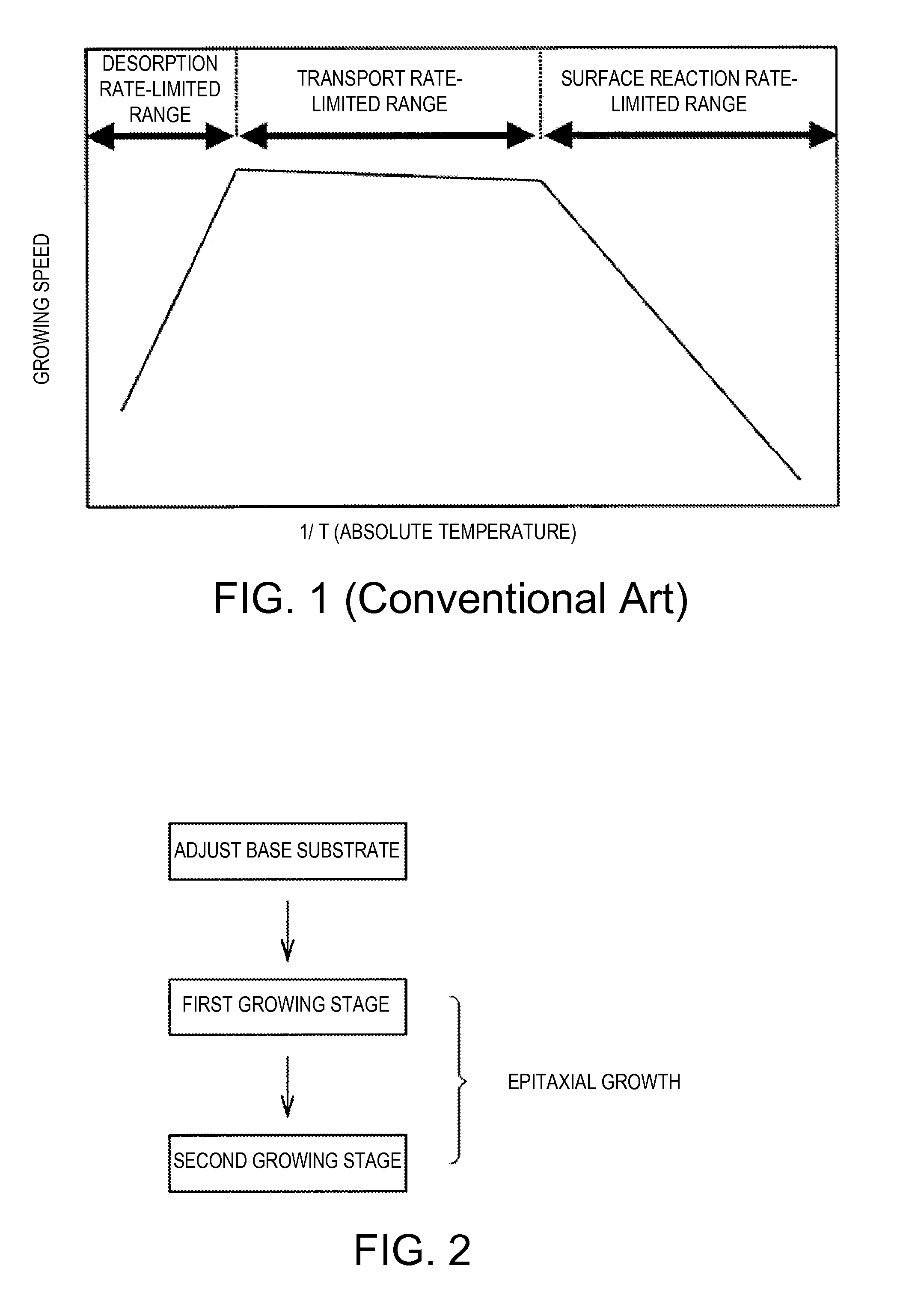
The existence of defects in single crystal SiC causes degradation of performance of single crystal SiC when it is used as the semiconductor device, and even when it is used as a foundation substrate of a GaN layer, causes a degradation of a quality of the GaN layer.

Method used


Image

  • Method of manufacturing single crystal 3c-sic substrate and single crystal 3c-sic substrate obtained from the manufacturing method
  • Method of manufacturing single crystal 3c-sic substrate and single crystal 3c-sic substrate obtained from the manufacturing method
  • Method of manufacturing single crystal 3c-sic substrate and single crystal 3c-sic substrate obtained from the manufacturing method

Examples


examples

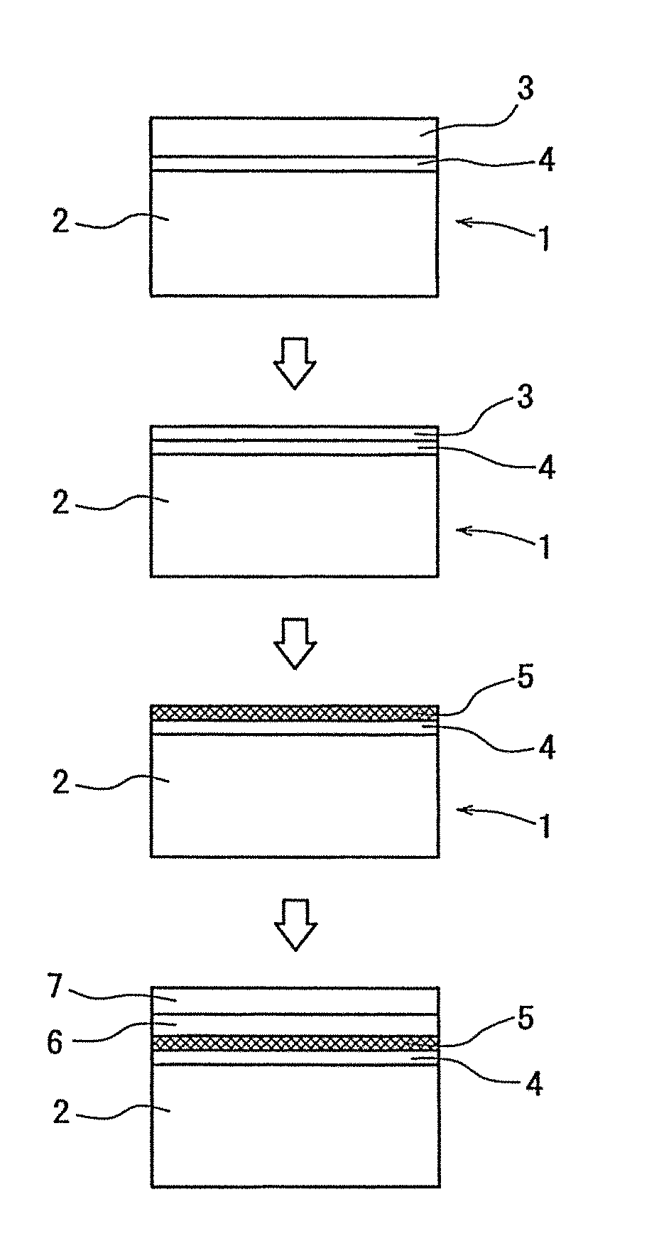
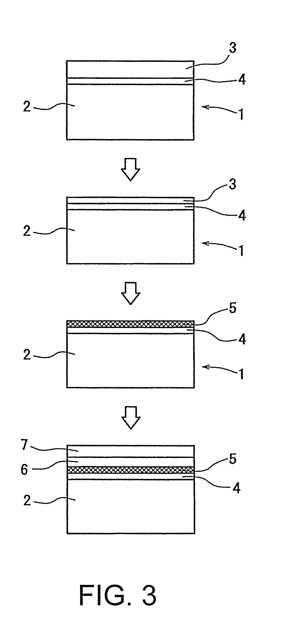
[0146]Next, examples of manufacturing the single crystal 3C-SiC substrate of the present invention are described.

[0147]An SOI substrate and an Si substrate are prepared as base substrates, and adjustments of the base substrates are performed under the following conditions, respectively.

♦ SOI Substrate

[0148]Substrate Thickness: 725 μm

[0149]Surface Si layer Thickness: 11 to 25 μm

[0150]Embedded Insulating Layer Thickness: 100 to 200 nm

[0151]Carbonization Condition: atmosphere gas is propane and hydrogen (carrier gas), temperature is 1200 to 1405° C., and time is 10 to 30 minutes

[0152]Single Crystal 3C-SiC Seed Layer Thickness: 5 to 7 nm

♦ Si Substrate

[0153]Substrate Thickness: 500 to 1000 μm

[0154]Carbonization Conditions: atmosphere gas is propane and hydrogen (carrier gas), propane: hydrogen=1:100, temperature is 1200 to 1405° C., and time is 10 to 30 minutes

[0155]Single Crystal 3C-SiC Seed Layer Thickness: 5 to 7 nm

[0156]Subsequently, a single crystal 3C-SiC layer is grown by the epit...


PUM

PropertyMeasurementUnit
pressureaaaaaaaaaa
pressureaaaaaaaaaa
temperatureaaaaaaaaaa

Abstract

To provide a method of manufacturing a single crystal 3C-SiC substrate that can dramatically reduce surface defects generated in a processing of epitaxial growth and can secure a quality as a semiconductor device while simplifying a post process. The method of manufacturing a single crystal 3C-SiC substrate where a single crystal 3C-SiC layer is formed on a base substrate by epitaxial growth is provided. A first growing stage of forming the single crystal 3C-SiC layer to have a surface state configured with a surface with high flatness and surface pits scattering in the surface is performed. A second growing stage of further epitaxially growing the single crystal 3C-SiC layer obtained in the first growing stage so as to fill the surface pits is performed.

Description

TECHNICAL FIELD[0001]The present invention relates to a method of manufacturing a single crystal 3C (cubic system)-SiC substrate that can dramatically reduce surface defects, and relates to a single crystal 3C-SiC substrate obtained from the manufacturing method.RELATED ART[0002]Single crystal SiC (silicon carbide) excels in thermal and chemical stability, is high in mechanical strength, and is not damaged easily from irradiation of radioactive rays. Due to these properties, it has attracted attention as a semiconductor device material for the next generation. Further, single crystal SiC has a close number of lattice constant to GaN, and thus, it can also be used as foundation substrates where GaN is grown.[0003]Conventionally, as methods of obtaining single crystal SiC, methods of obtaining SiC bulk substrates obtained from the sublimation method and methods of heteroepitaxially growing single crystal 3C-SiC on an Si substrate or an SOI substrate have been performed. As for the met...

Claims


Application Information

Patent Timeline
Patent Type & Authority Applications(United States)
IPC IPC(8): C30B25/16C30B29/36C30B25/14
CPCC30B25/02C30B29/36H01L21/0237H01L21/02447Y10T428/24355H01L21/02529H01L21/02614H01L21/0262H01L21/02661H01L21/02494C30B25/16C30B25/20H01L21/20
Inventor ASAMURA, HIDETOSHIKAWAMURA, KEISUKEOBARA, SATOSHI
Owner AIR WATER INC
Why Eureka
Try Eureka