

In-Line Photoluminescence Imaging of Semiconductor Devices
a technology of photoluminescence imaging and semiconductor devices, applied in the direction of luminescent dosimeters, fluorescence/phosphorescence, optical radiation measurement, etc., can solve the problems of adding cost, adding cost, and requiring samples to be taken to the imaging tool
- Summary
- Abstract
- Description
- Claims
- Application Information
AI Technical Summary
Benefits of technology
Problems solved by technology
Method used
Image

Examples
example 1
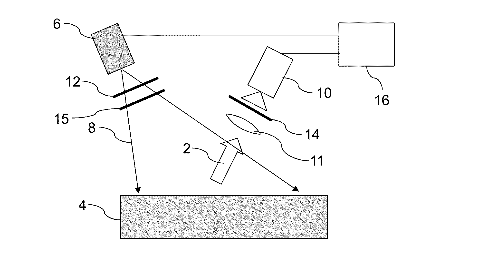
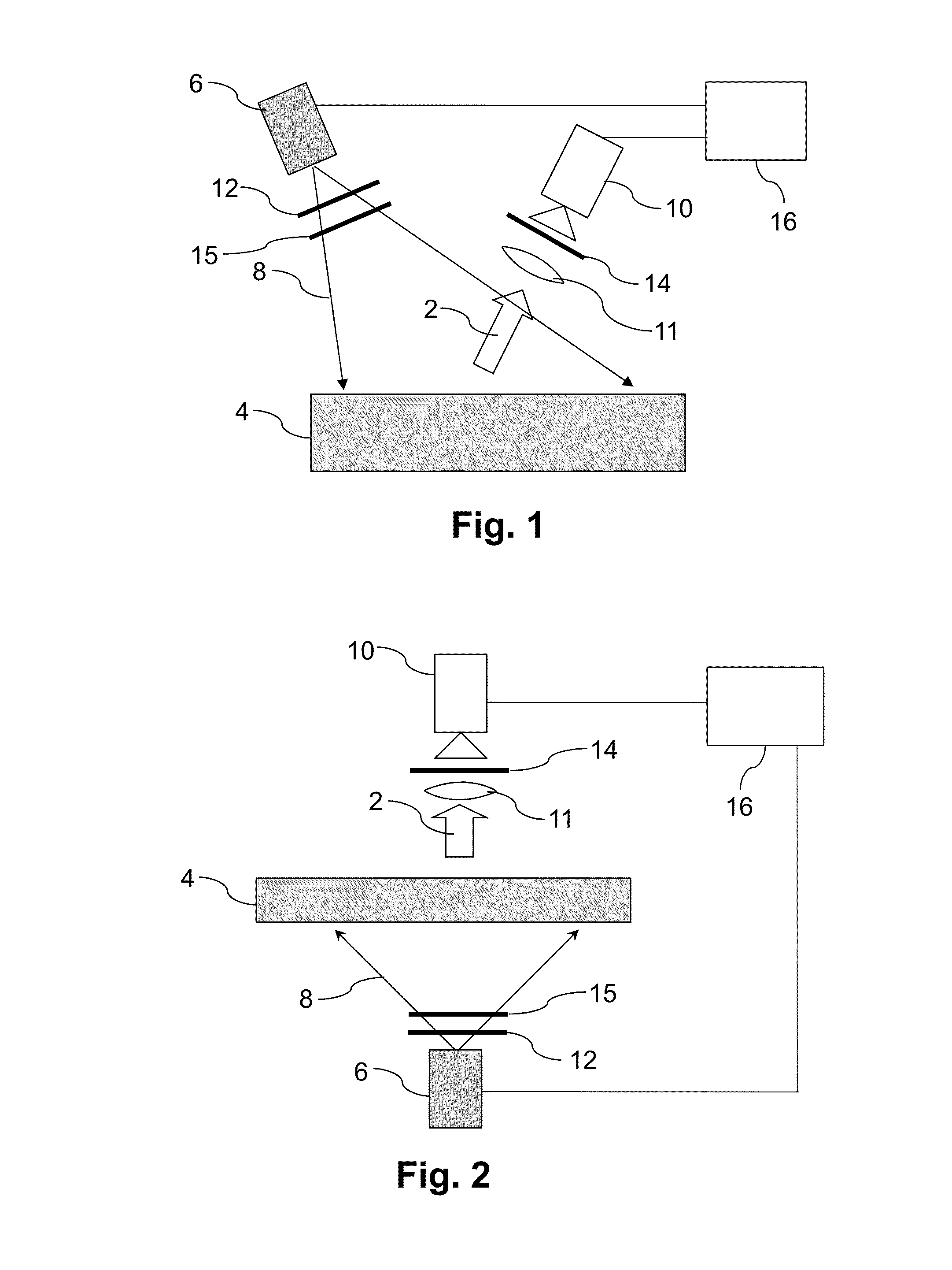
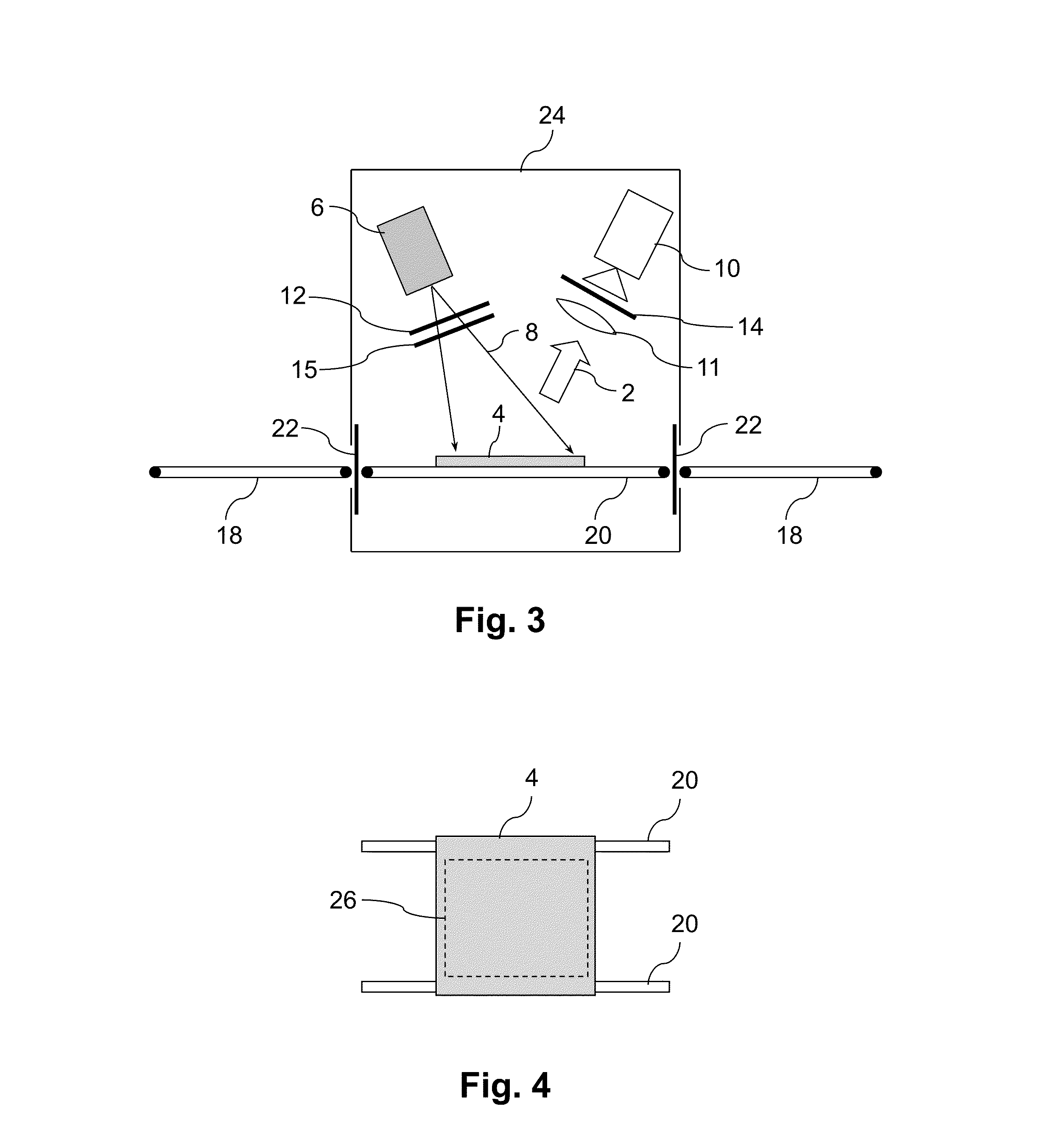
2D Area Imaging Geometry in Three-Belt System of FIG. 3 (Stationary Sample)
[0156]To incorporate a three-belt system into a solar cell line with a throughput of one cell per second, the measurement time clearly cannot exceed one second. To guarantee this for unpassivated samples it is necessary to achieve a thousand-fold increase in measurement speed. This could be done for example with a combination of:[0157]1) Si-CCD camera with 20×20 μm2 pixels (16× gain compared to the baseline example)[0158]2) F#=2 lens (2× gain)[0159]3) Illumination intensity of 1 W / cm2 i.e. 10 Suns (10× gain)[0160]4) 2×2 pixel binning (4× gain)
[0161]It will be appreciated that many other combinations are possible, e.g. 40 Suns illumination without pixel binning
example 2
Line Scan System with Line Illumination (165 μm Width and 156 mm Length) and Detection on Unpassivated Wafer
[0162]In this case a 1 ms measurement time per line is needed, requiring a 106 times increase in measurement speed compared to the Baseline Example. One possible combination is:[0163]1) InGaAs camera (20× gain)[0164]2) 25×25 μm2 pixels (25× gain)[0165]3) Illumination intensity of 1 W / cm2 i.e. 10 Suns (10× gain)[0166]4) Improved collection efficiency (200× gain)
[0167]It should be noted that because the illuminated area is much smaller than in the Baseline Example, it would be relatively straightforward to use much higher illumination intensities (hundreds of Suns) if collection efficiency improvements are more limited.
example 3
Line Scan System with Line (165 μm Width and 156 mm Length) Illumination and Detection on Passivated Multicrystalline Wafer
[0168]As for Example 2a 1 ms measurement time per line is needed, which in this case requires a 60,000 times increase in measurement speed compared to the Baseline Example. One possible combination is:[0169]1) Si-CCD camera with 20×20 μm2 pixels (16× gain)[0170]2) Illumination intensity of 2 W / cm2 i.e. 20 Suns (20× gain)[0171]3) Improved collection efficiency (200× gain)
[0172]Alternatively an InGaAs camera would give the required measurement speed if collection efficiency improvements are more limited, or if the PL intensity increases sub-linearly with illumination intensity.
PUM
| Property | Measurement | Unit |
|---|---|---|
| size | aaaaa | aaaaa |
| wavelengths | aaaaa | aaaaa |
| diameter | aaaaa | aaaaa |
Abstract
Description
Claims
Application Information