Etching liquid for a copper/titanium multilayer thin film

Active Publication Date: 2013-02-28
MITSUBISHI GAS CHEM CO INC +1
View PDF5 Cites 17 Cited by
  • Summary
  • Abstract
  • Description
  • Claims
  • Application Information

AI Technical Summary

Benefits of technology

[0013]According to the present invention, there are provided an etching liquid which secures, in an etching process for a multilayer thin film containing a copper layer and a titanium layer, high processing accuracy, little etching residue and unevenness and a long bath life, and realizes a good wiring profile after etching therewith, and which therefore can meet the requirement of size enlargement and

Problems solved by technology

However, with growing in size and increasing in resolution of displays, there has occurred a problem of RC delay caused by the characteristics such as the wiring resistance of such aluminium-based wiring materials and uniform panel displaying has tended to be difficult.
However, copper has an advantage in that its resistance is low but, on the other hand, has a problem in that, in use for gate wiring, t

Method used


Image

  • Etching liquid for a copper/titanium multilayer thin film
  • Etching liquid for a copper/titanium multilayer thin film

Examples


examples

[0034]Next, the present invention is described further in detail by Examples; however, the present invention is not whatsoever restricted by these Examples.

(Observation of Cross Section of Multilayer Thin Film Containing Copper Layer and Titanium Layer after Etching)

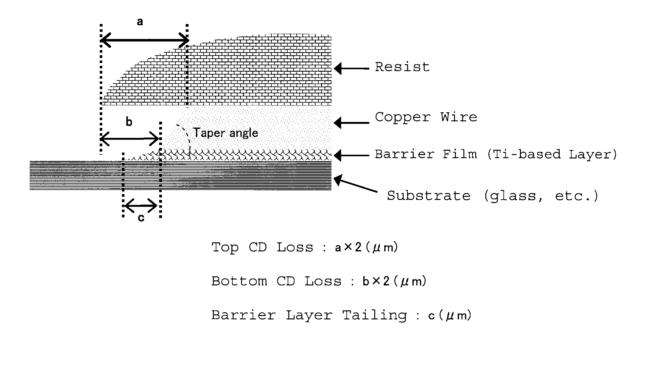
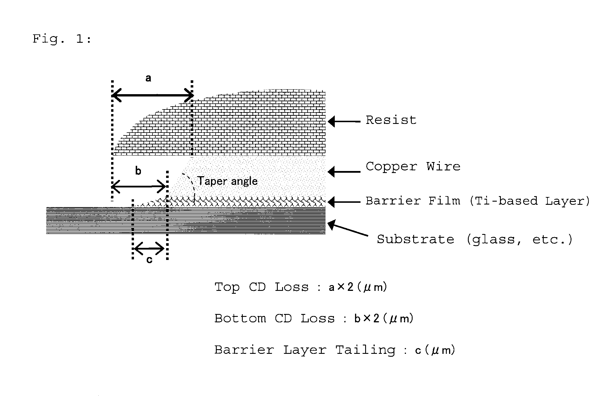
[0035]A sample of the etched multilayer thin film containing a copper layer and a titanium layer, as obtained in Examples and Comparative Examples, was cut and observed with a 50000 magnification through scanning electronic microscope (“S5000H

[0036]Type (Model Number)”, by Hitachi) (acceleration voltage 2 kV, acceleration current 10 μA). On the thus-taken SEM image, the taper angle, the top CD loss (μm), the bottom CD loss (μm) and the barrier film tailing (μm) as shown in FIG. 1 were determined.

[0037]Samples of which the taper angle, the top CD loss (μm), the bottom CD loss (μm) and the barrier film tailing (μm) each were within the standard range shown in Table 1 were considered to be good, and the performance of the e...

production example

Production of Multilayer Thin Film Containing Copper Layer and Titanium Layer

[0040]Titanium (Ti) was sputtered onto a substrate of glass to thereby form a barrier film of titanium (titanium layer) thereon, then a copper-based material was sputtered thereonto to form a wiring material film (copper layer), then a resist was applied onto it, a pattern mask was transferred through exposure thereonto, and developed to form a wiring pattern, thereby producing a multilayer thin film containing a copper layer and a titanium layer in which the copper layer was laminated on the titanium layer.

examples 1 to 10

[0041]The multilayer thin film containing a copper layer and a titanium layer, as produced in Production Example, was etched with the etching liquid shown in Table 2, at 35° C. for 60 to 150 seconds, thereby giving an etched, multilayer thin film sample containing a copper layer and a titanium layer, and the amount of the metal dissolved in the etching liquid was measured. Thus processed, the sample was analyzed according to the above-mentioned method to measure the taper angle, the top CD loss (μm), the bottom CD loss (μm) and the barrier film tailing (μm) in the initial bath. In case where the data in this stage still fell within the standard range in Table 1, still another new multilayer thin film containing a copper layer and a titanium layer was etched in the bath, and this process was repeated here. At the time when any of these numerical data came to fall outside the standard range in Table 1, the etching treatment was finished. The amount of the metal dissolved in the etchin...


PUM

PropertyMeasurementUnit
Percent by massaaaaaaaaaa

Abstract

The present invention provides an etching liquid for a multilayer thin film containing a copper layer and a titanium layer, and a method of using it for etching a multilayer thin film containing a copper layer and a titanium layer, that is, an etching liquid for a multilayer thin film containing a copper layer and a titanium layer, which comprises (A) hydrogen peroxide, (B) nitric acid, (C) a fluoride ion source, (D) an azole, (E) a quaternary ammonium hydroxide and (F) a hydrogen peroxide stabilizer and has a pH of from 1.5 to 2.5, and a etching method of using it.

Description

TECHNICAL FIELD[0001]The present invention relates to an etching liquid for a multilayer thin film containing a copper layer and a titanium layer, and to an etching method using it. In particular, the etching liquid of the present invention is favorably used for etching of a multilayer thin film having a copper layer provided on a titanium layer.BACKGROUND ART[0002]Heretofore, aluminium or an aluminium alloy has been generally used as the wiring material for display devices such as flat panel displays, etc. However, with growing in size and increasing in resolution of displays, there has occurred a problem of RC delay caused by the characteristics such as the wiring resistance of such aluminium-based wiring materials and uniform panel displaying has tended to be difficult.[0003]Given the situation, the recent tendency is toward investigation of employing copper or copper-based wiring with a material having a lower resistance. However, copper has an advantage in that its resistance i...

Claims


Application Information

Patent Timeline
IPC IPC(8): C23F1/10
CPCC23F1/18C23F1/26C23F1/44H01L21/32134H01L2924/0002H01L23/53238H05K3/067H01L2924/00H01L21/308H01L21/3213
Inventor ADANIYA, TOMOYUKIOKABE, SATOSHIGOTOU, TOSHIYUKIMARUYAMA, TAKETOKOBAYASHI, KAZUKITANAKA, KEIICHINAKAMURA, WATARUKITOH, KENICHITANAKA, TETSUNORI
Owner MITSUBISHI GAS CHEM CO INC
Why Eureka
Try Eureka