Semiconductor light emitting device including metal reflecting layer

Active Publication Date: 2013-02-28
NICHIA CORP
View PDF3 Cites 39 Cited by
  • Summary
  • Abstract
  • Description
  • Claims
  • Application Information

AI Technical Summary

Benefits of technology

[0014]To solve the above object, a semiconductor light emitting device according to a first aspect of the present invention includes a semiconductor structure 11, a transparent electrically-conducting layer 13, a dielectric film 4, and a metal reflecting layer 22. The semiconductor structure 11 includes an active region 8. The transparent electrically-conducting layer 13 is formed on or above the upper surface of the semiconductor structure 11. The dielectric film 4 is formed on or above the upper surface of the transparent electrically-conducting layer 13. The metal reflecting layer 22 is formed on or above the upper surface of the dielectric film 4. The dielectric film 4 has at least one opening 21 whereby partially exposing the transparent electrically-conducting layer 13. The transparent electrically-conducting layer 13 is electrically connected to the metal reflecting layer 22 through the openin

Problems solved by technology

However, in this construction, since a reflecting structure 3020 is used which includes the dielectric film 304 made from metal, (i.e., electrically-conductive reflecting layer), the electrically conductive reflecting structure may cause undesirable electrical connection in a part where electrical insulation is poor, for example, in an exposed part on the end surface, or in a part where the electrically insulating film is poorly formed.
Consequently, it is unavoidable that a non-covered part that is not covered by the reflecting structure 3020 is formed in the light emitting device.
In this case, there is a problem that light cannot effectively extract. FIG. 32 shows reflection of light from a light-emitting layer 308 in the light

Method used


Image

  • Semiconductor light emitting device including metal reflecting layer
  • Semiconductor light emitting device including metal reflecting layer
  • Semiconductor light emitting device including metal reflecting layer

Examples


first embodiment

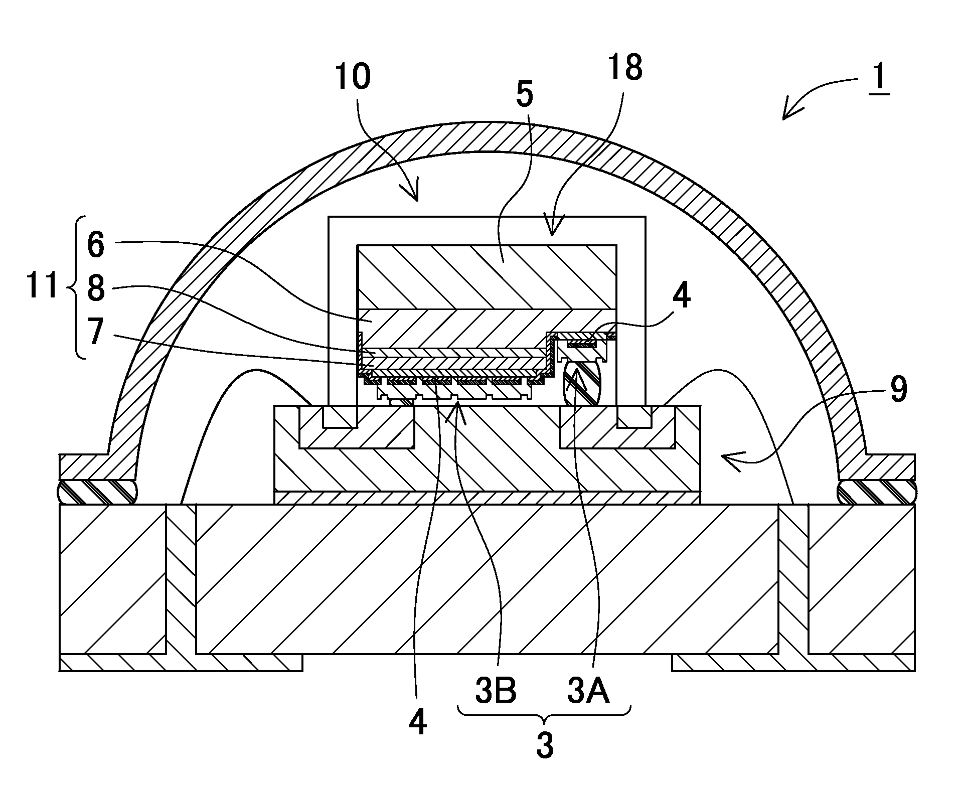
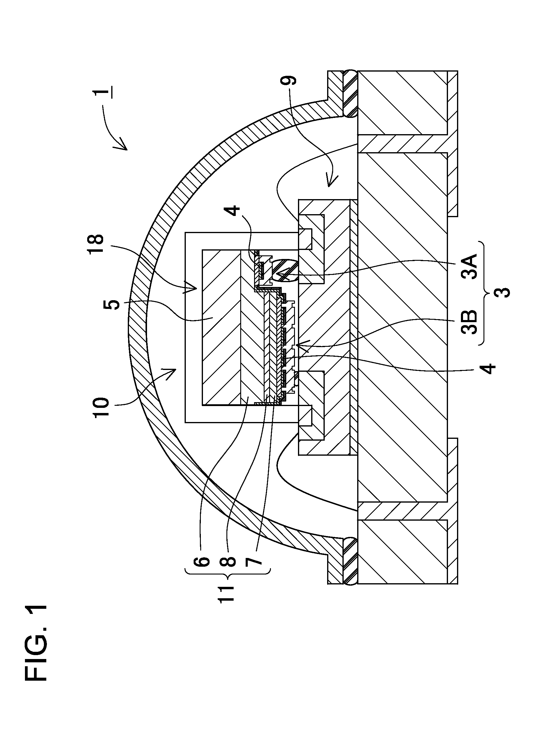
[0067]FIG. 1 is a cross-sectional view showing a light emitting apparatus 1 according to a first embodiment of the present invention. This illustrated light emitting apparatus 1 includes a light emitting device 10 of an LED chip as an exemplary nitride semiconductor device. This LED chip is mounted onto a wiring board 9, which is a sort of submount, in a flip-chip mounting manner. The flip-chip mounting manner refers to a mounting manner where a growth substrate 5 serves as a main light extraction surface through which light outgoes. Semiconductor layers are deposited on the growth substrate. The growth substrate 5 is opposed to an electrode formation surface on which an electrode is formed. The flip-chip mounting manner is also referred to as facedown mounting manner. The light emitting device 10 is shown upside down in FIG. 1 for illustrating the flip-chip mounting manner.

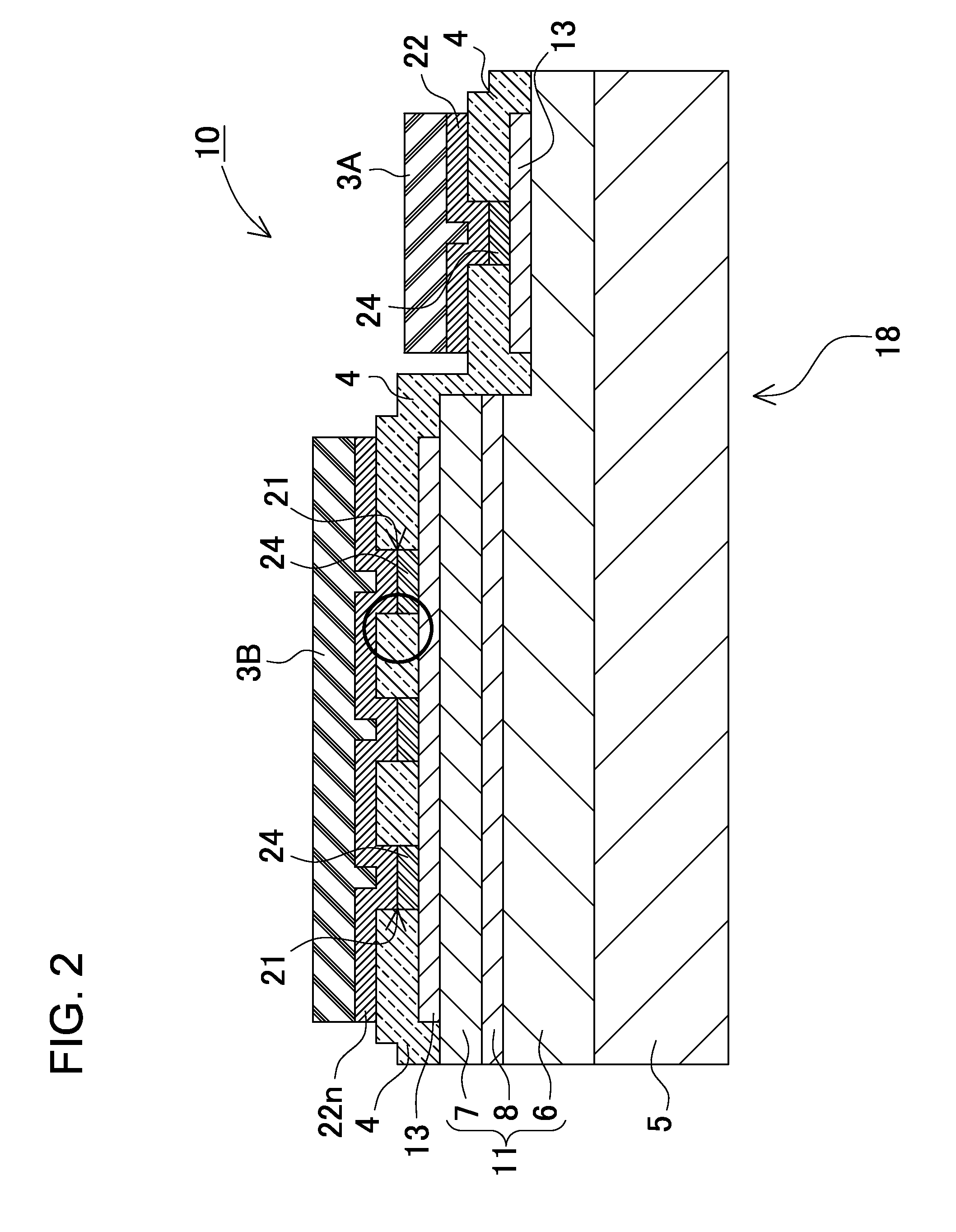
[0068]FIG. 2 is a cross-sectional view schematically showing the light emitting device 10 shown in FIG. 1 befo...

second embodiment

[0099]An eutectic-bonding pad electrode can be additionally arranged on the pad electrode. FIGS. 4 to 7 show a light emitting device 10′ according to a second embodiment that includes the eutectic-bonding pad electrode. FIG. 4 is a schematic cross-sectional view showing the light emitting device 10′. FIGS. 5 to 7 show exemplary construction of the light emitting device 10′ according to the second embodiment. FIG. 5 is a plan view showing the light emitting device 10′. FIG. 6A is a cross-sectional view of the light emitting device 10′ shown in FIG. 5 taken along the line VI-VI. FIG. 7 is a cross-sectional view of the light emitting device 10′ shown in FIG. 5 taken along the line VII-VII. The illustrated semiconductor light emitting device 10′ has substantially the same construction as the light emitting device shown in FIG. 2. Components of semiconductor light emitting device 10′ same as those of the light emitting device shown in FIG. 2 are attached with the same reference signs, an...

third embodiment

[0105]The semiconductor light emitting device can have a gap between the pad electrodes, which are provided for external connection. FIG. 9 shows this type of semiconductor light emitting device 10″ according to a third embodiment. The production method of the semiconductor light emitting device according to the third embodiment is now described with reference to a flowchart of FIG. 10, and cross-sectional views of FIGS. 11A to 11E and 12F to 12I. The cross-sectional views show a die for ease of illustration. Illustration of the dividing process is omitted which divides a wafer into chips after wafer processes for the sake of brevity. Main processes can be shown as follows:

Step S1: Epitaxial Growth

Step S2: Exposure of N-Type Layer

Step S3: Formation of ITO Ohmic Electrode

Step S4: Formation of DBR Film on Whole Surface

Step S5: Formation of Resist Mask for Forming Openings

Step S6: DBR Film Dry Etching

Step S7: Formation of Barrier Metal Film

Step S8: Liftoff

Step S7: Formation of Pad Elec...


PUM


Abstract

A semiconductor light emitting device includes a semiconductor structure, a transparent electrically-conducting layer, a dielectric film, and a metal reflecting layer. The semiconductor structure includes an active region. The transparent electrically-conducting layer is formed on the upper surface of the semiconductor structure. The dielectric film is formed on the upper surface of the transparent electrically-conducting layer. The metal reflecting layer is formed on the upper surface of the dielectric film. The dielectric film has at least one opening whereby partially exposing the transparent electrically-conducting layer. The transparent electrically-conducting layer is electrically connected to the metal reflecting layer through the opening. A barrier layer is partially formed and covers the opening so that the barrier layer is interposed between the transparent electrically-conducting layer and the metal reflecting layer.

Description

BACKGROUND OF THE INVENTION[0001]1. Field of the Invention[0002]The present invention relates to a semiconductor light emitting device.[0003]2. Description of the Related Art[0004]Semiconductor light emitting devices can be small and highly effective in power consumption, and can emit vivid color light. In addition, in the case of light emitting devices of semiconductor elements, there are no concerns about bulb burnout and the like. In addition, semiconductor light emitting devices have features such as excellent driven characteristics, resistance to vibration or ON / OFF repeats. Since semiconductor light emitting devices have these excellent features, semiconductor light emitting devices such as light emitting diode (hereinafter, occasionally referred to as “LED”) and laser diode (hereinafter, occasionally referred to as “LD”) have been used as various types of light sources. In particular, in recent years, light emitting diodes receive attention as light source for lighting replac...

Claims


Application Information

Patent Timeline
IPC IPC(8): H01L33/60
CPCH01L33/38H01L33/44H01L33/42H01L33/405H01L33/02H01L33/10H01L33/46H01L2224/16145H01L2224/48091H01L2224/73265H01L2924/00014
Inventor KUSUSE, TAKESHIAZUMA, NAOKIOGAWA, TOSHIAKIKASAI, HISASHI
Owner NICHIA CORP
Why Eureka
Try Eureka