

Vertically foldable memory array structure
a memory array and vertical folding technology, applied in semiconductor devices, digital storage, instruments, etc., can solve the problems of vertical series sonos flash memory process and control method, conventional planar nand array flash memory may not be endlessly scaled down, etc., to improve a high-density and large-capacity merit, simple and flexible, and simple structure
- Summary
- Abstract
- Description
- Claims
- Application Information
AI Technical Summary
Benefits of technology
Problems solved by technology
Method used
Image

Examples
embodiment 1
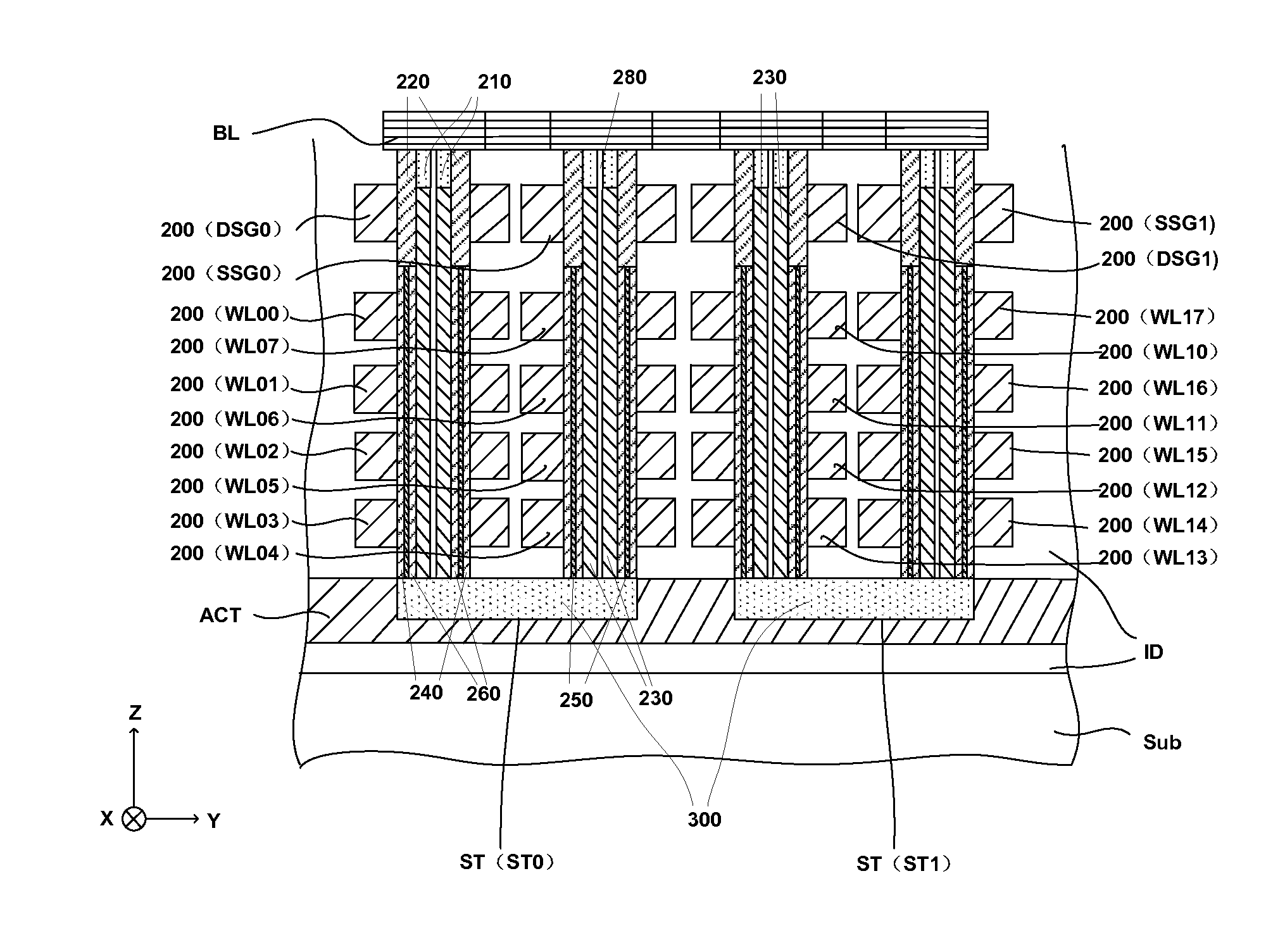
[0041]In some embodiments of the present disclosure, the vertically foldable memory array structure comprises: a memory module distributed in columns and rows, the memory module comprising: a drain selection transistor; a bottom connecting line and a source selection transistor; and a plurality of memory cell transistors connected between the drain selection transistor and the bottom connecting line and between the source selection transistor and the bottom connecting line, in which a gate in each of the plurality of memory cell transistors is connected to a word line, a drain of each drain selection transistor is connected to a bit line, a drain of a drain selection transistor in a Mth vertically foldable memory module in a Nth column and a source of a source selection transistor in a (M−1)th memory module in a (N+1)th column are connected to a same bit line, gates of the drain selection transistors and the source selection transistors in all the memory modules in the Nth column ar...
embodiment 2
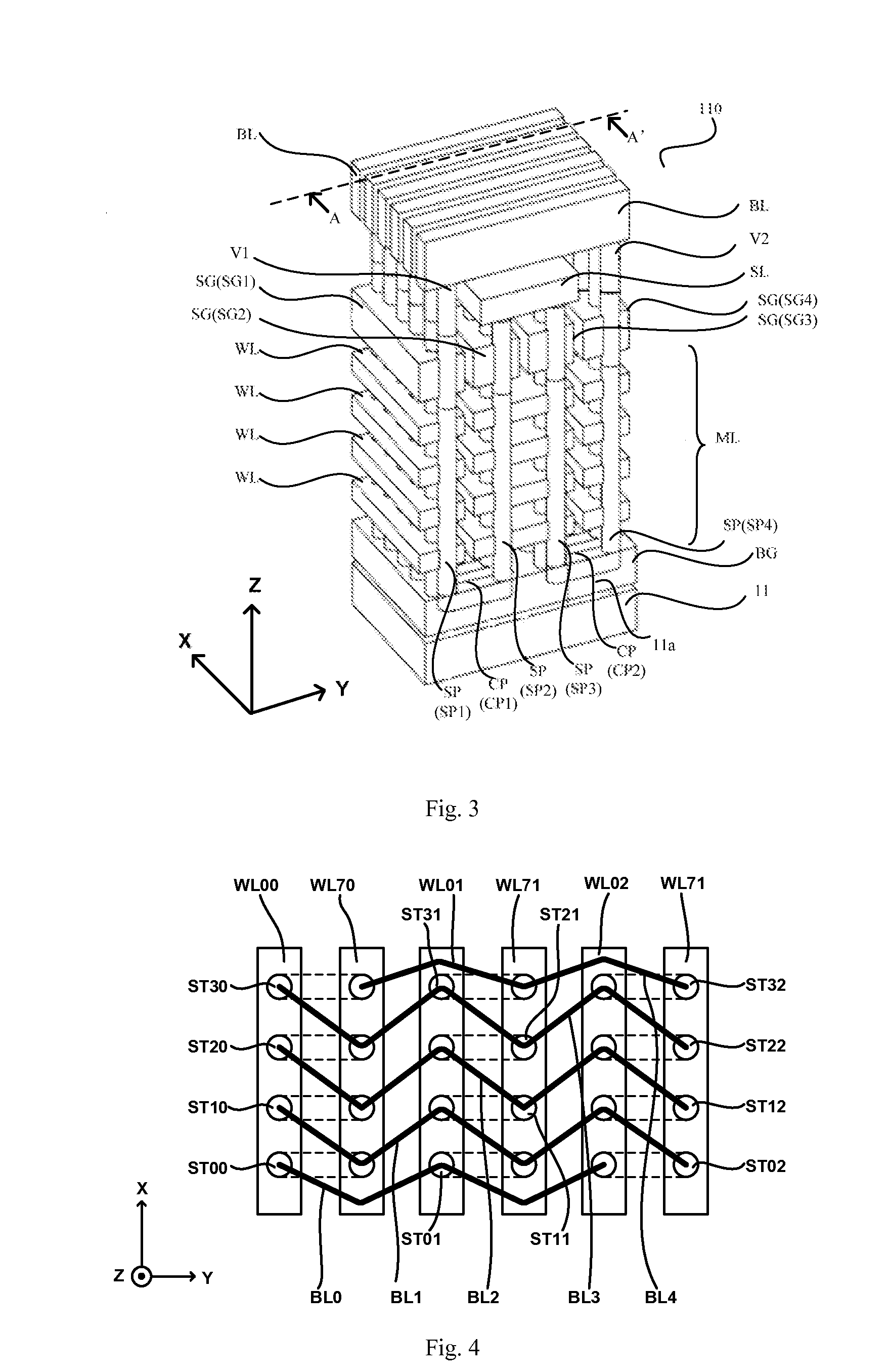
[0058]The vertically foldable memory array structure according to a second embodiment of the present disclosure comprises: a memory cell transistor set distributed in columns and rows and comprising a plurality of memory cell transistors, in which a gate of each memory cell transistor is connected to a word line; a plurality of drain selection transistors and a plurality of source selection transistors, in which each of the memory cell transistor sets in a Nth column is connected to one drain selection transistor, and each of the memory cell transistor sets in a (N+1)th column is connected to one source selection transistor; and a plurality of bottom connecting lines connected between a memory cell transistor set in a Mth row and in the Nth column and a memory cell transistor set in a (M+1)th row and in the (N+1)th column, in which a drain of a drain selection transistor and a source of a source selection transistor corresponding to the memory cell transistor set in each row are con...
PUM
 Abstract
Description
Claims
Application Information