Method for producing semiconductor device and semiconductor device

a semiconductor device and semiconductor technology, applied in the direction of semiconductor devices, basic electric elements, electrical appliances, etc., can solve the problems of difficult to stop etching with good controllability, difficult to form a thick mask layer, etc., to achieve stable operation of semiconductor devices, high integration, and high speed driving

Active Publication Date: 2013-03-21
UNISANTIS ELECTRONICS SINGAPORE PTE LTD
View PDF2 Cites 17 Cited by
  • Summary
  • Abstract
  • Description
  • Claims
  • Application Information

AI Technical Summary

Benefits of technology

[0045]According to a method for producing a semiconductor device and a semiconductor device according to the present invention, an upper region and a lower region of a pillar-shaped semiconductor that forms a circuit element can be easily connected to a wiring layer arranged above the pillar-shaped semiconductor, and high integration, high-speed driving, and stable operation of a semiconductor device including a circuit element can be realized.

Problems solved by technology

Furthermore, in the case where such two contact holes are formed at the same time, in terms of manufacturing, it may be difficult to stop etching with good controllability on the surfaces of a semiconductor layer and a conductor layer by reactive ion etching (RIE) or the like.
Furthermore, in the case where two contact holes are formed at the same time, it is difficult to form a thick mask layer for etching such as RIE so as to form a deep contact hole, to remove the mask layer for etching after the RIE etching, and, furthermore, to remove etching residue.

Method used


Image

  • Method for producing semiconductor device and semiconductor device
  • Method for producing semiconductor device and semiconductor device
  • Method for producing semiconductor device and semiconductor device

Examples


first embodiment

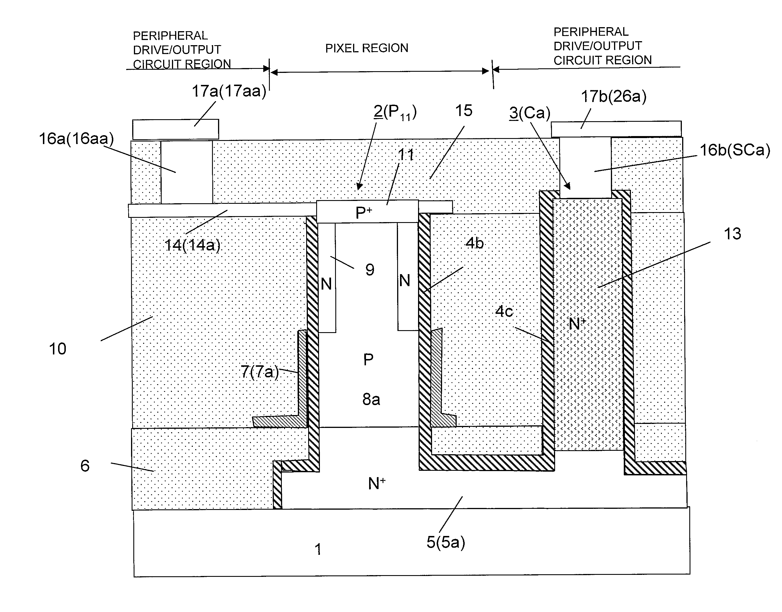
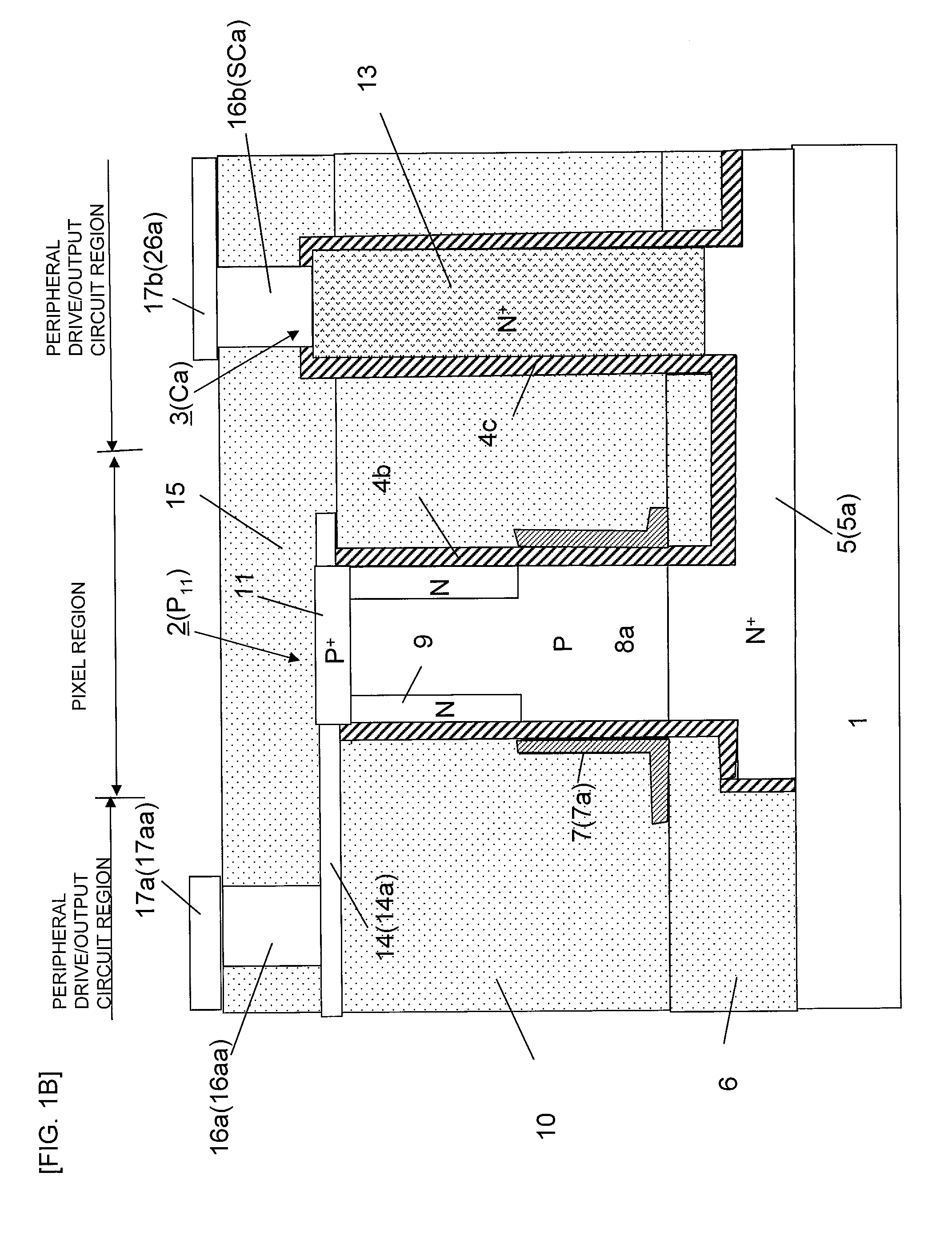
[0099]A solid-state imaging device according a first embodiment of the present invention, and a method for producing the solid-state imaging device will now be described with reference to FIGS. 1A, 1B, and 2A to 2F.

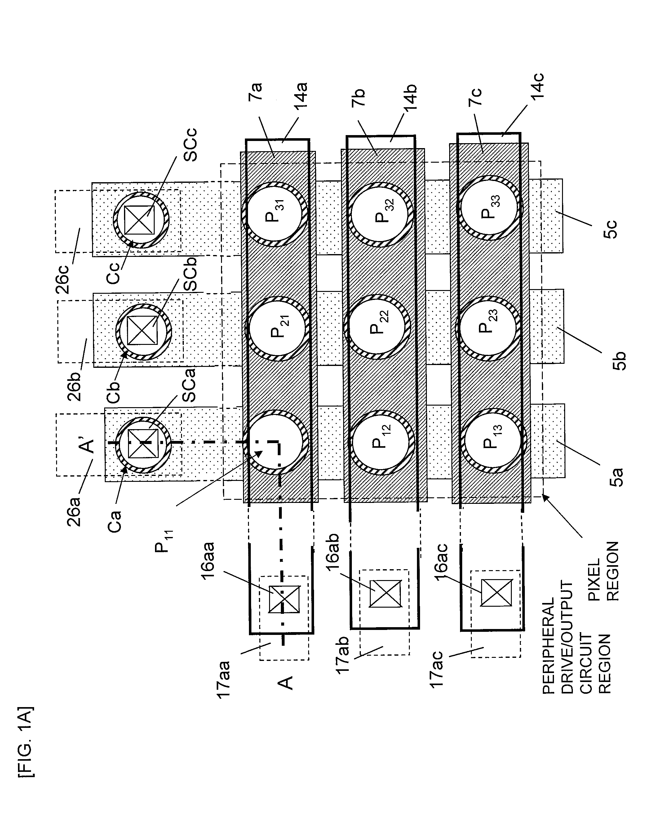
[0100]FIG. 1A is a plan view of a solid-state imaging device according to this embodiment. In a pixel region of the solid-state imaging device, silicon pillars P11 to P33 that form pixels are arranged in a vertical (column) direction and a horizontal (row) direction two-dimensionally (in a matrix). These silicon pillars P11 to P33 are formed on signal line N+ layers 5a, 5b, and 5c that are formed on a silicon oxide substrate 1 and that extend in the vertical (column) direction of the figure and to a peripheral drive / output circuit region. The signal line N+ layers 5a, 5b, and 5c are respectively connected to signal line metal layers 26a, 26b, and 26c through contact holes SCa, SCb, and SCc that are respectively formed on second silicon pillars Ca, Cb, and Cc in the periph...

second embodiment

[0114]FIGS. 3A to 3C illustrate a method for producing a solid-state imaging device according to this embodiment. In this embodiment, the electrical resistance between a signal line N+ layer 5 and a signal line metal layer 17b is decreased by forming a silicide layer 23 instead of the conductor N+ layer 13 of the second silicon pillar 3 that establishes contact in FIG. 1B.

[0115]In this embodiment, first, the steps illustrated in FIGS. 2A to 2D in the first embodiment are performed. Subsequently, as illustrated in FIG. 3A, a pixel selection line conductor layer 14 connected to a P+ layer 11 of a first silicon pillar 2 is formed. A SiO2 layer 18 and a photoresist layer 19 are formed by CVD, and a through-hole 20 is formed on a second silicon pillar 3 by photolithography and etching. Subsequently, as illustrated in FIG. 3A, an impurity such as silicon (Si) or hydrogen (H), which does not function as a donor or an acceptor, is introduced into the second silicon pillar 3 by ion implantat...

third embodiment

[0119]A method for producing a solid-state imaging device according to this embodiment will now be described with reference to FIGS. 4A to 4D and FIG. 5. In this embodiment, the resistance between a signal line N+ layer 5 and a signal line metal layer 73b is decreased by forming a metal layer 70a or 70b composed of tungsten (W), copper (Cu), or the like instead of the conductor N+ layer 13 of the second silicon pillar 3 that establishes contact in FIG. 1B.

[0120]In this embodiment, first, the steps illustrated in FIGS. 2A to 2C in the first embodiment are performed. Subsequently, as illustrated in FIG. 4A, an N layer 9 that forms a photodiode is formed on an outer peripheral portion of a first silicon pillar 2. A Si nitride (SiN) layer 64 is formed on the first silicon pillar 2, a second silicon pillar 3, and a SiO2 layer 6 by CVD. Subsequently, as illustrated in FIG. 4A, the whole structure is covered with a SiO2 layer 65, and the surface of the SiO2 layer 65 is polished by chemical...


PUM


Abstract

A method for producing a semiconductor device includes the steps of forming first and second pillar-shaped semiconductors on a substrate at the same time so as to have the same height; forming a first semiconductor layer by doping a bottom region of the first pillar-shaped semiconductor with a donor or acceptor impurity to connect the first semiconductor layer to the second pillar-shaped semiconductor; forming a circuit element including an upper semiconductor region formed by doping an upper region of the first pillar-shaped semiconductor with a donor or acceptor impurity; forming a first conductor layer in the second pillar-shaped semiconductor; forming first and second contact holes that are respectively connected to the first and second pillar-shaped semiconductors; and forming a wiring metal layer that is connected to the upper semiconductor region and the first conductor layer through the first and second contact holes, respectively.

Description

RELATED APPLICATIONS[0001]Pursuant to 35 U.S.C. §119(e), this application claims the benefit of the filing date of Provisional U.S. Patent Application Ser. No. 61 / 535,133 filed on Sep. 15, 2011. The entire content of this application is hereby incorporated by reference.BACKGROUND OF THE INVENTION[0002]1. Field of the Invention[0003]The present invention relates to a semiconductor device and a method for producing a semiconductor device, and in particular, to a method for producing a semiconductor device including a transistor in which a channel region is formed in a semiconductor having a pillar structure, and the semiconductor device.[0004]2. Description of the Related Art[0005]Realization of higher performance has been desired in, for example, CMOS solid-state imaging devices in which a pixel is formed in a pillar-shaped semiconductor or in semiconductor devices in which a MOS transistor is formed in a pillar-shaped semiconductor.[0006]Solid-state imaging devices are widely used i...

Claims


Application Information

Patent Timeline
Patent Type & Authority Applications(United States)
IPC IPC(8): H01L29/78H01L21/336
CPCH01L21/84H01L27/1203H01L29/78642
Inventor MASUOKA, FUJIOHARADA, NOZOMU
Owner UNISANTIS ELECTRONICS SINGAPORE PTE LTD
Why Eureka
Try Eureka