Thin film forming method and film forming apparatus

a film forming method and film forming technology, applied in the direction of polycrystalline material growth, crystal growth process, chemically reactive gas, etc., can solve the problem of insufficient embedding characteristic, and achieve the effect of satisfying the embedding characteristic and improving the precision of surface roughness

Active Publication Date: 2013-04-04
TOKYO ELECTRON LTD
View PDF13 Cites 25 Cited by
  • Summary
  • Abstract
  • Description
  • Claims
  • Application Information

AI Technical Summary

Benefits of technology

[0014]To solve the above problems, the present invention provides a thin film forming method and a film forming apparatus which are capable of forming a thin film, such as a silicon film or a silicon germanium film, which has a satisfactory embedding characteristic even at a relatively low temperature and improves a precision of surface roughness.

Problems solved by technology

However, when the design rule is strict due to a recent increased request for further minuteness, a sufficient embedding characteristic may not be obtained.

Method used


Image

  • Thin film forming method and film forming apparatus
  • Thin film forming method and film forming apparatus
  • Thin film forming method and film forming apparatus

Examples


an embodiment

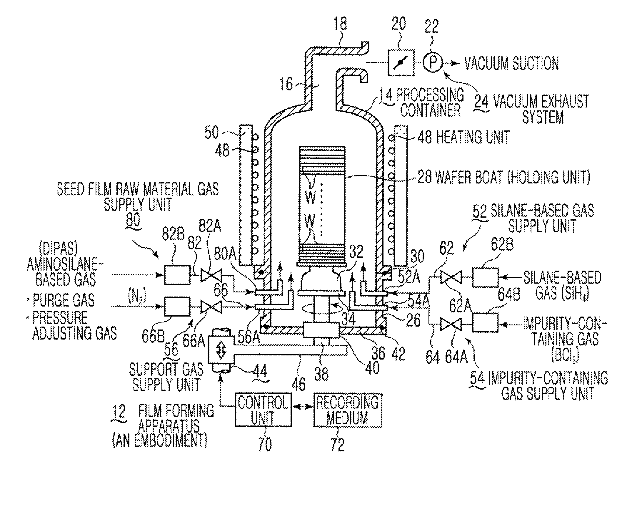
[0044]FIG. 1 is a structural view showing an example of an embodiment of a film forming apparatus for performing a film forming method of the present invention. Throughout the drawings, like reference numerals denote like elements. As shown, the film forming apparatus 12 includes a batch-type vertical processing container 14 having a shape of a bottom-open cylinder. The processing container 14 may be formed of, for example, quartz having a high thermal resistance.

[0045]An opened exhaust port 16 is provided at a ceiling portion of the processing container 14 while an exhaust nozzle 18, for example, perpendicularly curved in a horizontal direction, is continuously provided from the exhaust port 16. Also, since a vacuum exhaust system 24 including a pressure control valve 20 or a vacuum pump 22 is connected to the exhaust nozzle 18, an atmosphere in the processing container 14 may be vacuum-sucked and exhausted.

[0046]A bottom of the processing container 14 is supported by a manifold 26...

modified example

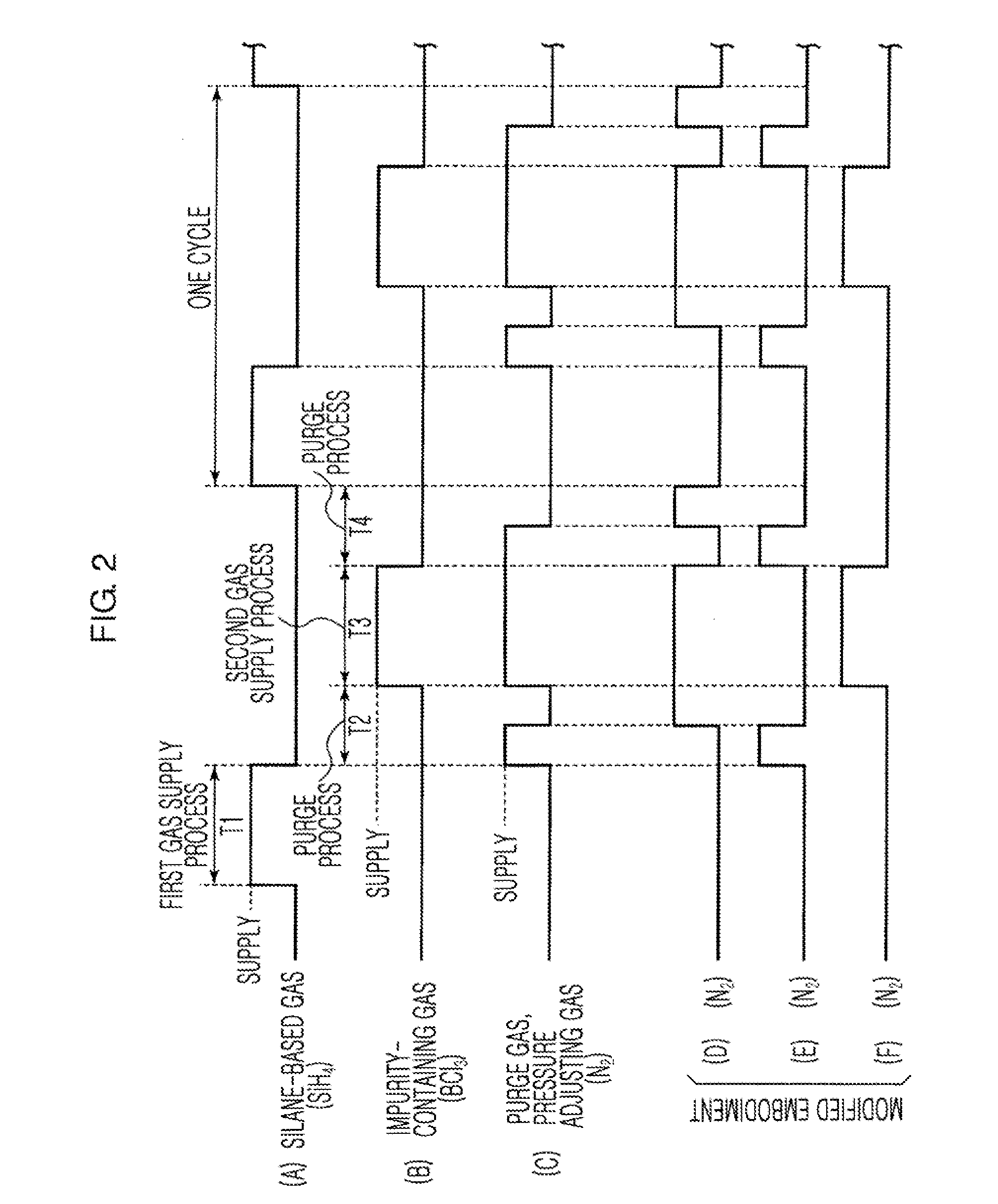
[0109]In the above embodiments, the silane-based gas and the impurity-containing gas are alternately supplied in the second step, but alternatively, the silane-based gas and the impurity-containing gas may be simultaneously supplied to form an impurity-containing silicon film via a CVD method. In this case, regarding process conditions, a flow rate of the silane-based gas (for example, monosilane), is in a range from 100 to 2000 sccm and a flow rate of the impurity-containing gas (for example, BCl3) is in a range from 50 to 2000 sccm. Also, a process pressure is in a range from 0.1 to 10 Torr and a process temperature is in a range from 350 to 600° C. Also, a process time is determined based on a film thickness required. The same effects as the above embodiments may be obtained in the modified example.

[0110]2) and Existence of Seed Film>

[0111]Next, the results of evaluating a type of a base (insulation film 2) and the existence of a seed film will now be described. Here, according t...

modified example 1

[0140]In the above embodiment, the silane-based gas and the germanium-containing gas, and the impurity-containing gas are alternately supplied in the second step, but alternatively, the silane-based gas and the germanium-containing gas, and the impurity-containing gas may be simultaneously supplied to form an impurity-containing SiGe film via a CVD method. In this case, regarding process conditions, a flow rate of the silane-based gas (for example, monosilane) is in a range from 100 to 2000 sccm, a flow rate of the germanium-containing gas (for example, monogermane) is in a range from 100 to 2000 sccm, and a flow rate of the impurity-containing gas (for example, BCl3) is in a range from 50 to 500 sccm. Also, a process pressure is in a range from 0.1 to 10 Torr and a process temperature is in a range from 350 to 600° C. Also, a process time is determined based on a film thickness required. In this case, the same effects as the above embodiment may be obtained.


PUM

PropertyMeasurementUnit
thicknessaaaaaaaaaa
temperatureaaaaaaaaaa
temperaturesaaaaaaaaaa

Abstract

A thin film forming method which forms a seed film and an impurity-containing silicon film on a surface of an object to be processed in a processing container configured to be vacuum exhaustible includes: performing a first step which forms the seed film by supplying a seed film raw material gas including at least any one of an aminosilane-based gas and a higher silane into the processing container; and performing a second step which forms the impurity-containing silicon film in an amorphous state by supplying a silane-based gas and an impurity-containing gas into the processing container.

Description

CROSS-REFERENCE TO RELATED PATENT APPLICATIONS[0001]This application claims the benefits of Japanese Patent Application No. 2011-217390, filed on Sep. 30, 2011 and Japanese Patent Application No. 2011-240840, filed on Nov. 2, 2011 in the Japan Patent Office, the disclosures of which are incorporated herein in its entirety by reference.BACKGROUND OF THE INVENTION[0002]1. Field of the Invention[0003]The present invention relates to a film forming method and film forming apparatus, which form a seed film and a thin film on a surface of an object to be processed, such as a semiconductor wafer.[0004]2. Description of the Related Art[0005]Generally, in order to manufacture a semiconductor integrated circuit, various processes, such as a film forming process, an etching process, an oxidation process, a diffusion process, a modification process, and a natural oxide film removing process, are performed on a semiconductor wafer including a silicon substrate, etc. The film forming process is d...

Claims


Application Information

Patent Timeline
Patent Type & Authority Applications(United States)
IPC IPC(8): H01L21/205H01L21/20
CPCC23C16/24C30B25/02C30B29/06H01L21/67109C23C16/045C23C16/45523C23C16/0272H01L21/205H01L21/02167H01L21/02271H01L21/02312
Inventor KAKIMOTO, AKINOBUENDO, ATSUSHIMIYAHARA, TAKAHIRONAKAJIMA, SHIGERUTAKAGI, SATOSHIIGARASHI, KAZUMASA
Owner TOKYO ELECTRON LTD
Why Eureka
Try Eureka