Method of manufacturing semiconductor device

a manufacturing method and semiconductor technology, applied in the direction of semiconductor devices, electrical devices, transistors, etc., can solve the problems of increasing the voltage of the element, increasing the diffusion time so as to reduce the breakdown voltage, reduce the diffusion time, and reduce the diffusion time. effect of required to form the isolation region through silicon

Inactive Publication Date: 2013-05-16
FUJI ELECTRIC CO LTD
View PDF5 Cites 22 Cited by
  • Summary
  • Abstract
  • Description
  • Claims
  • Application Information

AI Technical Summary

Benefits of technology

[0026]In addition, in the subsequent cooling process, when the temperature of the wafer is in the range of 300° C. to 500° C., the crystal defect in the wafer serves as a donor and the impurity concentration of the drift region is changed. This problem is more noticeable as the breakdown voltage of the element increases. The reason is that, as the breakdown voltage increases, the thickness of the drift region increases, which results in an increase in the diffusion time required to form the isolation region. Therefore, the breakdown voltage is reduced or the amount of leakage current increases. As a result, the performance or reliability of the reverse blocking IGBT is reduced and yield is likely to be significantly reduced.
[0077]According to the method of manufacturing a semiconductor device of the invention, it is possible to form the diffusion region which extends from the first main surface to the second main surface of the wafer for a short diffusion time. In addition, it is possible to provide a method of manufacturing a semiconductor device with a high breakdown voltage. It is possible to reduce costs.

Problems solved by technology

The inventors conducted intensive studies and found that the following problems occurred in the isolation region forming method according to the related art.
This problem is more noticeable as the breakdown voltage of the element increases.
The reason is that, as the breakdown voltage increases, the thickness of the drift region increases, which results in an increase in the diffusion time required to form the isolation region.
As a result, the performance or reliability of the reverse blocking IGBT is reduced and yield is likely to be significantly reduced.
In this case, a wafer cost increases in correspondence with the improvement in the performance.

Method used


Image

  • Method of manufacturing semiconductor device
  • Method of manufacturing semiconductor device
  • Method of manufacturing semiconductor device

Examples


first embodiment

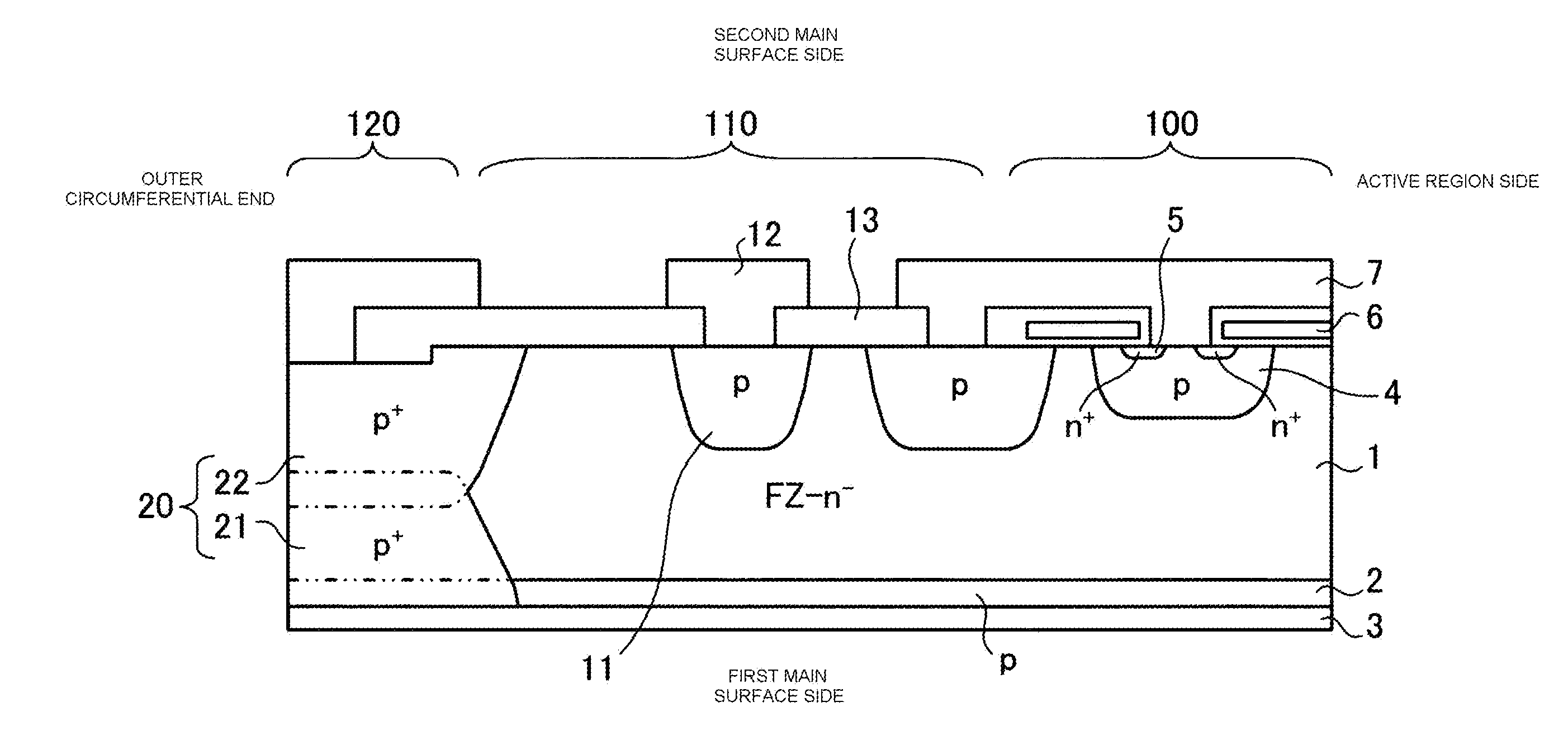
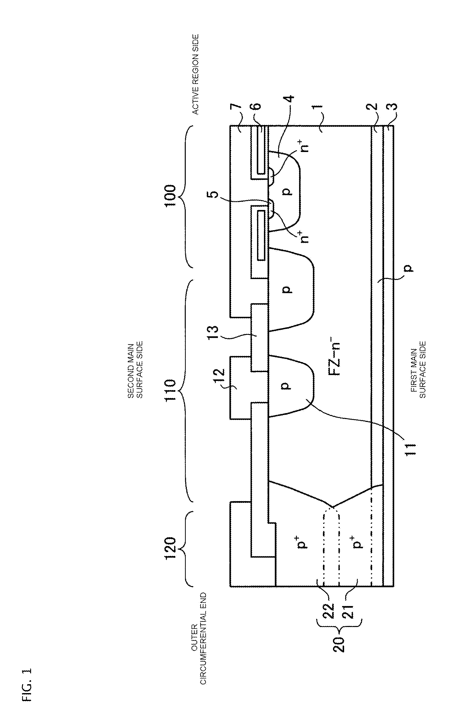
[0112]FIG. 1 is a cross-sectional view illustrating a reverse blocking IGBT according to a first embodiment. The reverse blocking IGBT shown in FIG. 1 includes an n− (first conduction type) wafer (second wafer) 1 which becomes a drift region, active region 100, and breakdown voltage structure 110 which surrounds active region 100. It is preferable that, for example, a silicon wafer (hereinafter, referred to as an FZ wafer) manufactured by a floating zone (FZ) method be used as wafer 1. P collector region 2 which is a p type (second conduction type) is provided on the entire first main surface of wafer 1. A collector electrode 3 comes into contact with p collector region 2.

[0113]In active region 100, for example, a surface element structure of a planar-gate-type IGBT including p base region 4, n+ emitter region 5, gate electrode 6, and emitter electrode 7 is formed on the second main surface of wafer 1. Breakdown voltage structure 110 includes a plurality of field limiting rings 11, ...

second embodiment

[0151]FIG. 14 is a cross-sectional view illustrating a reverse blocking IGBT according to a second embodiment. An n− epitaxial layer may be provided between the n− drift region and the p collector region of the reverse blocking IGBT according to the first embodiment.

[0152]In the reverse blocking IGBT shown in FIG. 14, an n− epitaxial layer 8 is provided between an n− wafer (first wafer) 1 which is a drift region and p collector region 2. Through silicon isolation region 70 includes first isolation region 71 and second isolation region 72. First isolation region 71 is provided so as to extend from a surface layer of the first main surface of wafer 1 to epitaxial layer 8. In addition, first isolation region 71 comes into contact with p collector region 2 at the end close to CZ wafer 84 and comes into contact with second isolation region 72 at the end close to the second main surface of FZ wafer 1. Second isolation region 72 is provided in the surface layer of the second main surface o...


PUM


Abstract

Mirror-polished CZ wafer and FZ wafer are prepared. A first impurity region which will be a first isolation region is formed in a surface layer of a first main surface of the CZ wafer. The first main surface of the CZ wafer and a first main surface of the FZ wafer are bonded to each other by an inter-molecular bond. A second impurity region which will be a second isolation region is formed in a surface layer of a second main surface of the FZ wafer. A heat treatment is performed to diffuse the first impurity region and the second impurity region such that the first impurity region and the second impurity region are continuous, thereby forming a through silicon isolation region.

Description

BACKGROUND OF THE INVENTION[0001]A. Field of the Invention[0002]The present invention relates to a method of manufacturing a semiconductor device.[0003]B. Description of the Related Art[0004]A discrete semiconductor with a high breakdown voltage plays an important role in a power conversion device. For example, an insulated gate bipolar transistor (IGBT) or an insulated gate field effect transistor (MOSFET) has been known as a discrete semiconductor. In particular, since the IGBT has the property that an on voltage is reduced by conductivity modulation, it is applied to a case in which power conversion is required at a high voltage.[0005]In recent years, a reverse blocking IGBT (RB-IGBT) has been developed which has a termination structure in which a high breakdown voltage (hereinafter, referred to as a reverse breakdown voltage) is obtained when a reverse bias is applied to a pn junction including a collector region and a drift region of the IGBT. For example, the reverse blocking ...

Claims


Application Information

Patent Timeline
Patent Type & Authority Applications(United States)
IPC IPC(8): H01L29/66
CPCH01L29/66333H01L29/7395H01L29/0834H01L29/0623H01L29/0661H01L29/0619
Inventor LU, HONG-FEI
Owner FUJI ELECTRIC CO LTD
Why Eureka
Try Eureka