
Negative pattern forming process

a negative pattern and forming technology, applied in the field of pattern forming process, can solve the problems of low resist resistance etching resistance, difficult to reduce the feature size of the hole pattern, and high cost of scanner

Active Publication Date: 2013-05-23
SHIN ETSU CHEM IND CO LTD
View PDF10 Cites 17 Cited by
  • Summary
  • Abstract
  • Description
  • Claims
  • Application Information

AI Technical Summary

Benefits of technology

The patent describes a method for creating fine patterns on a surface without creating a layer of retained material underneath. This is achieved by using a specific polymer, a PAG and an organic solvent in a process called organic solvent negative development. The technique allows for greater flexibility in the formation of patterns and can improve the resolution and accuracy of the final result.

Problems solved by technology

However, for the reasons that the projection lens uses a large amount of expensive CaF2 single crystal, the scanner thus becomes expensive, hard pellicles are introduced due to the extremely low durability of soft pellicles, the optical system must be accordingly altered, and the etch resistance of resist is low; the development of F2 lithography was stopped and instead, the ArF immersion lithography was introduced.
As compared with the line pattern, the hole pattern is difficult to reduce the feature size.
This, however, results in the exposure margin being extremely narrowed.
With the hole shrinking method, the hole size can be shrunk, but the pitch cannot be narrowed.
Although a hole pattern can be formed at a wide margin by combining X and Y lines and using dipole illumination featuring a high contrast, it is difficult to etch vertically staged line patterns at a high dimensional accuracy.
However, the crosslinking negative resist film has the drawback that the resolving power is low as compared with the positive resist film, because the maximum resolution of ultrafine holes is determined by the bridge margin.
However, the negative development in organic solvent is generally low in dissolution contrast, as compared with the positive development in alkaline aqueous solution.

Method used


Image

  • Negative pattern forming process
  • Negative pattern forming process
  • Negative pattern forming process

Examples


example

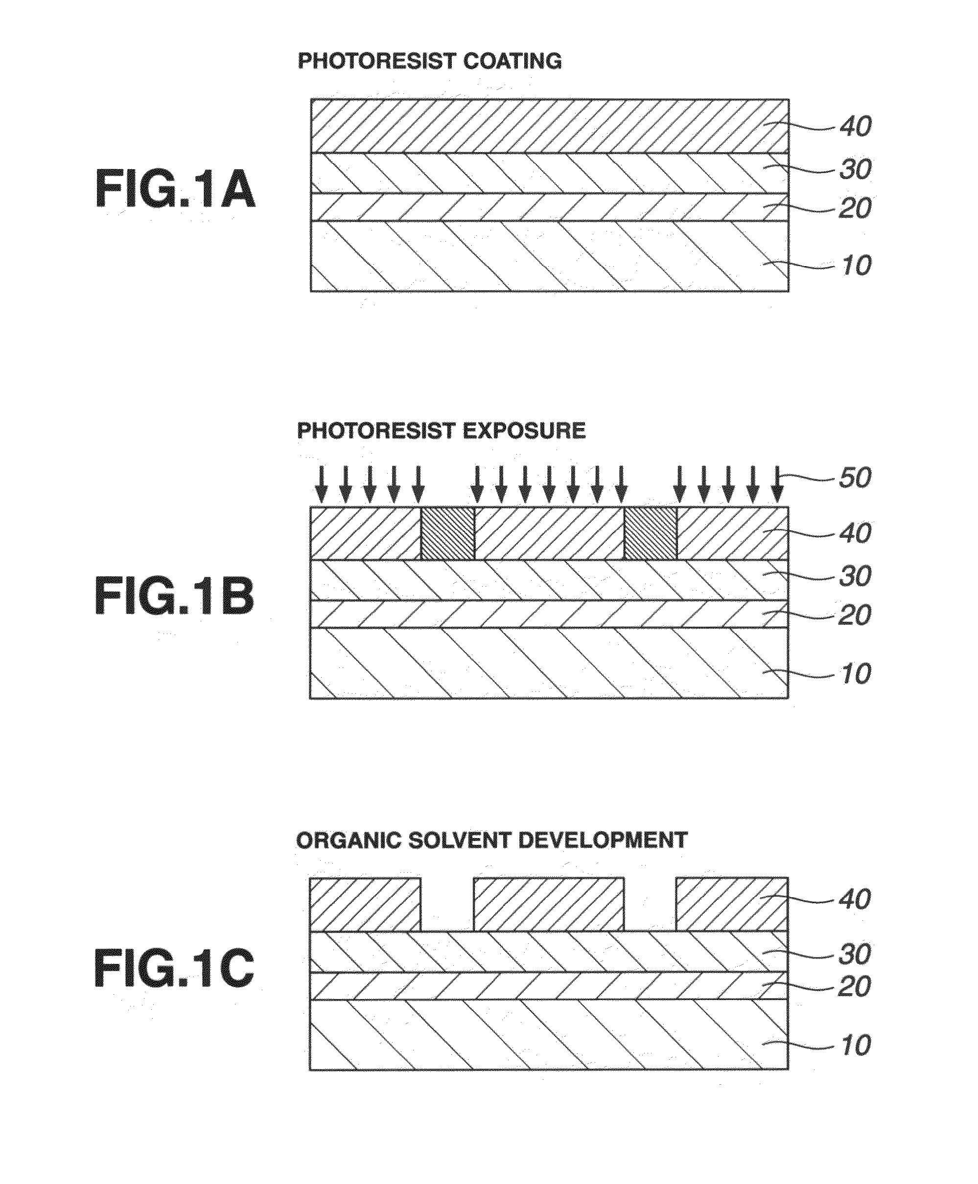
[0151]Examples of the invention are given below by way of illustration and not by way of limitation. The abbreviation “pbw” is parts by weight. For all polymers, Mw and Mn are determined by GPC versus polystyrene standards using tetrahydrofuran solvent.

Preparation of Resist Composition

[0152]Resist compositions in solution form (Resists 1 to 15) within the scope of the invention were prepared by dissolving components in a solvent in accordance with the recipe shown in Table 1, and filtering through a Teflon® filter with a pore size of 0.2 μm. Similarly, comparative resist compositions (Resists 16 to 18) outside the scope of the invention were prepared. Polymers 1 to 18 as base resin in Tables 1 and 2 have a structure, molecular weight (Mw) and dispersity (Mw / Mn) as shown in Tables 3 to 5. In Tables 3 to 5, the value in parentheses indicates a molar fraction (mol %) of the relevant recurring unit.

[0153]Polymeric additives PA-1 to 3 in Tables 1 and 2 were added for providing the resist...


PUM

PropertyMeasurementUnit
Percent by massaaaaaaaaaa
Wavelengthaaaaaaaaaa

Abstract

A negative pattern is formed by applying a resist composition comprising (A) a polymer comprising recurring units (a1) having a carboxyl group protected with an acid labile group and recurring units (a2) having an amino group, amide bond, carbamate bond or nitrogen-containing heterocycle, (B) a photoacid generator, and (C) an organic solvent onto a substrate, prebaking, exposing, baking, and selectively dissolving an unexposed region of the resist film in an organic solvent-based developer.

Description

CROSS-REFERENCE TO RELATED APPLICATION[0001]This non-provisional application claims priority under 35 U.S.C. §119(a) on Patent Application No. 2011-251229 filed in Japan on Nov. 17, 2011, the entire contents of which are hereby incorporated by reference.TECHNICAL FIELD[0002]This invention relates to a pattern forming process involving application of a specific resist composition, exposure of the resist film, heating to induce deprotection reaction under the catalysis of an acid generated by a photoacid generator, and development in an organic solvent to dissolve the unexposed region, but not the exposed region of the resist film to form a negative tone pattern.BACKGROUND ART[0003]In the recent drive for higher integration and operating speeds in LSI devices, the pattern rule is made drastically finer. The photolithography which is currently on widespread use in the art is approaching the essential limit of resolution determined by the wavelength of a light source. As the light sourc...

Claims


Application Information

Patent Timeline
IPC IPC(8): G03F7/004
CPCG03F7/004C08F2220/343G03F7/2041G03F7/325C08F220/34C08F2220/387G03F7/38C08F2220/382C08F226/06C08F228/06G03F7/0382C08F2220/365C08F2220/385C08F226/10C08F228/02C08F220/36G03F7/0397C08F220/365G03F7/0045G03F7/038G03F7/26C08F220/343C08F220/382C08F220/385C08F220/387
Inventor KOBAYASHI, TOMOHIROKATAYAMA, KAZUHIROHATAKEYAMA, JUNFUNATSU, KENJITACHIBANA, SEIICHIRO
Owner SHIN ETSU CHEM IND CO LTD
Learn More