Composition for forming liquid crystal layer, liquid crystal display device, and method for producing liquid crystal display device

a liquid crystal display and liquid crystal technology, applied in the field of liquid crystal display devices, can solve the problems of reduced aperture ratio, reduced white luminance, and taken before alignment stabilization, and achieve excellent display quality

Inactive Publication Date: 2013-05-30
SHARP KK +1
View PDF1 Cites 5 Cited by
  • Summary
  • Abstract
  • Description
  • Claims
  • Application Information

AI Technical Summary

Benefits of technology

[0043]According to the composition for forming a liquid crystal layer of the present invention, a liquid crystal display device can be fabricated in which the generation of the image sticking based on a residual DC voltage is prevented. Also according to the liquid crystal display device of the present invention, since the generation of the image sticking based on a resid

Problems solved by technology

However, the MVA mode, since using ribs (protrusions), has a decreased aperture ratio and consequently has a drawback of a low white luminance.
Although it suffices if the arrangement intervals of the ribs are made sufficiently large in order to improve this drawback, since

Method used


Image

  • Composition for forming liquid crystal layer, liquid crystal display device, and method for producing liquid crystal display device
  • Composition for forming liquid crystal layer, liquid crystal display device, and method for producing liquid crystal display device
  • Composition for forming liquid crystal layer, liquid crystal display device, and method for producing liquid crystal display device

Examples


embodiment 1

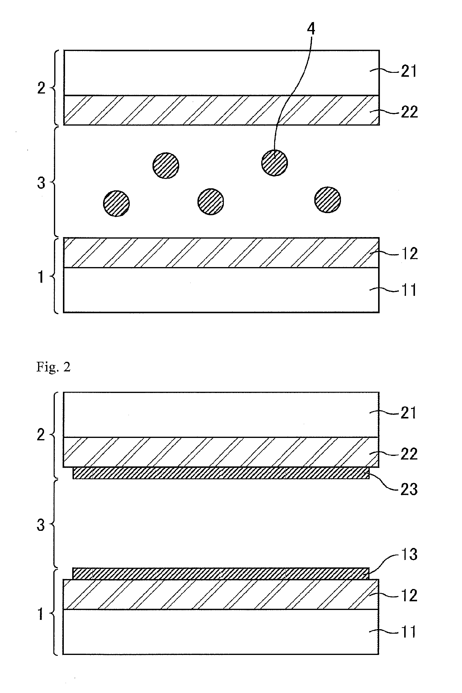
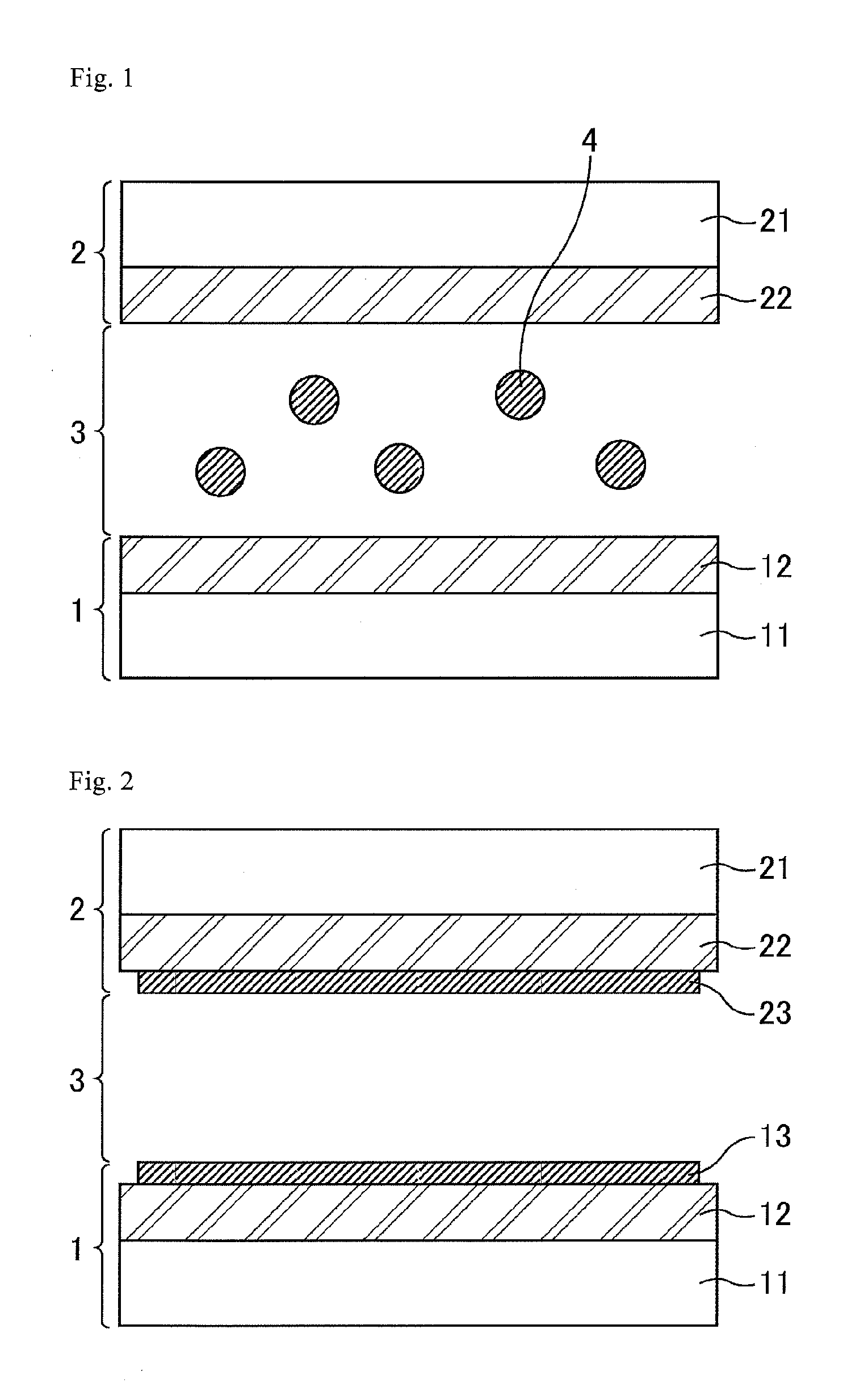
[0051]FIG. 1 and FIG. 2 are cross-sectional illustrative diagrams of a liquid crystal display device according to Embodiment 1. FIG. 1 shows one before the PSA polymerization step, and FIG. 2 shows one after the PSA polymerization step. As shown in FIG. 1 and FIG. 2, the liquid crystal display device according to Embodiment 1 has an array substrate 1, a color filter substrate 2 and a liquid crystal layer 3 interposed between a pair of substrates composed of the array substrate 1 and the color filter substrate 2. The array substrate 1 has a support substrate 11 having an insulating transparent substrate using a glass or the like as a material, and various types of wiring, pixel electrodes, TFTs (Thin Film Transistors) and the like formed on the transparent substrate. The color filter substrate 2 has a support substrate 21 having an insulating transparent substrate using a glass or the like as a material, and a color filter, a black matrix, common electrodes and the like formed on the...

example 1

[0067]Hereinafter, Example 1 will be shown in which liquid crystal cells which the liquid crystal display devices according to Embodiment 1 had were each actually fabricated. First, a pair of support substrates were prepared; and a polyamic acid solution being a material for a vertical alignment film was applied on the respective surfaces of the pair of support substrates, and pre-baked under a condition of 80° C. for 5 min, and then post-baked under a condition of 200° C. for 60 min.

[0068]Then, the alignment films after the post-baking were subjected to an alignment treatment. Then, a sealant was applied on the one substrate; and a composition for forming a liquid crystal layer containing a liquid crystal material having a negative anisotropy of dielectric constant and monomers for forming a PSA layer was dropped on the one substrate; and thereafter, the other substrate was laminated.

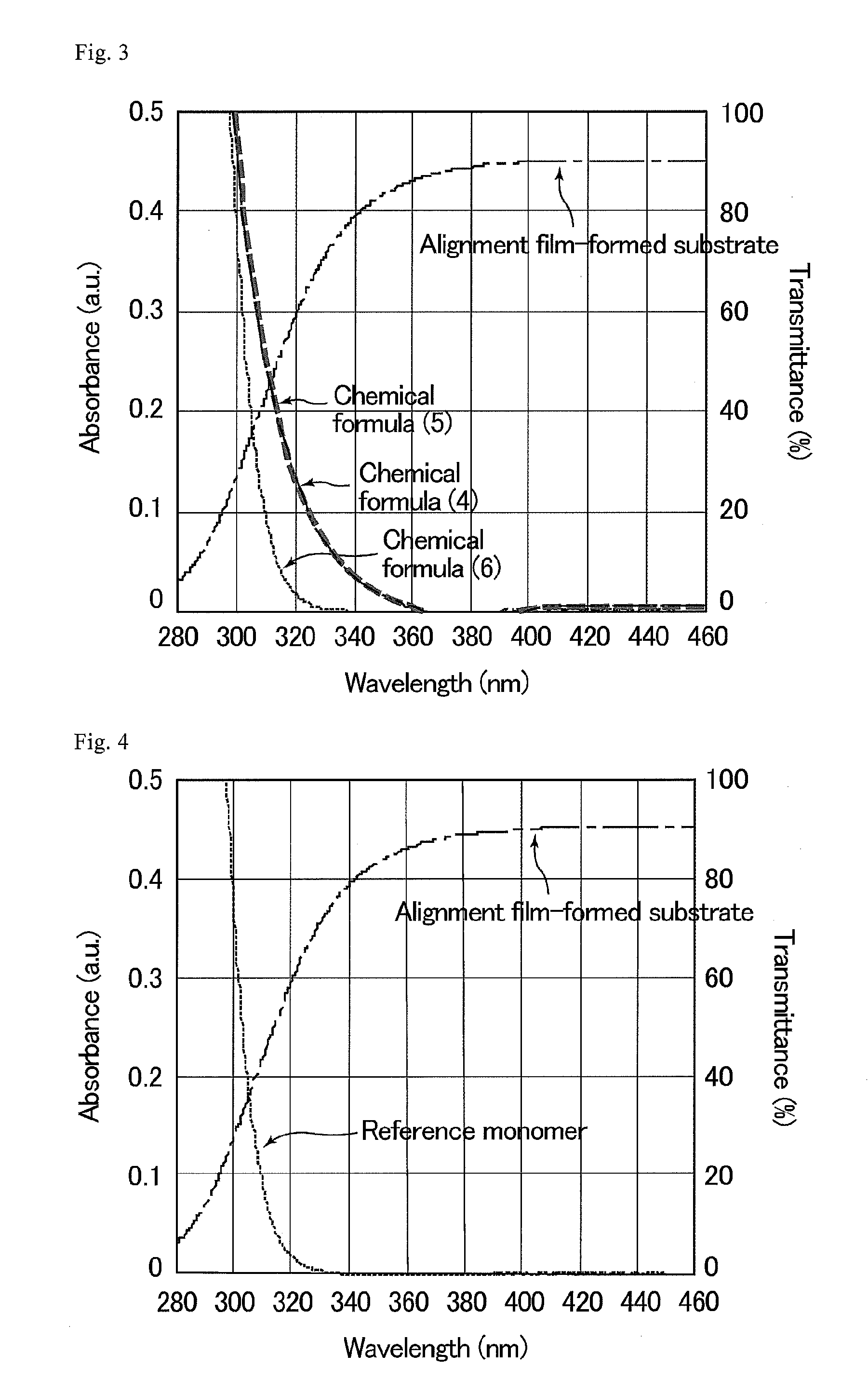
[0069]In Example 1, monomers are used as a combination of monomers represented by the following che...

synthesis example 1

Synthesis of 1,6-dimethacryloyloxyphenanthrene (the Above Chemical Formula (5)))

[Step 1] Synthesis of (4-bromobenzyl)triphenylphosphonium-bromide

[0071]8 g of 4-bromobenzyl bromide and 8.4 g of triphenylphosphine were dissolved in 194 g of toluene, and stirred at a reflux temperature for 4 hours. Thereafter, the stirred solution was cooled to 15° C., and a deposit was filtered. Thereafter, the filtered residue was washed with 16 g of cyclohexane, and further vacuum dried to thereby obtain 15.6 g of (4-bromobenzyl)triphenylphosphonium-bromide as a target. The reaction path herein is represented by the following chemical reaction formula (7).

[Step 2] Synthesis of 2,4′-dibromostilbene

[0072]15.6 g of the (4-bromobenzyl)triphenylphosphonium-bromide and 5.5 g of 2-bromobenzaldehyde were dissolved in 311 g of methylene chloride. Then, to the solution, 13.4 g of a 45%-NaOH aqueous solution was dropped over 30 min. After the dropping, the resultant solution was stirred at room temperature for...


PUM

PropertyMeasurementUnit
Electric potential / voltageaaaaaaaaaa
Compositionaaaaaaaaaa

Abstract

The present invention provides a composition for forming a liquid crystal layer from which a liquid crystal display device hardly generating image sticking can be obtained. The composition for forming a liquid crystal layer according to the present invention contains a liquid crystal material and one or two or more monomers, wherein at least one of the monomers is a phenanthrene derivative represented by the following chemical formula (1):
the following chemical formula (2):
or the following chemical formula (3):
wherein R1 and R2 are identical or different, and each denote an -Sp-P group, a hydrogen atom, a halogen atom, a —CN group, a —NO2 group, a —NCO group, a —NCS group, an —OCN group, a —SCN group, a —SF5 group, or a straight-chain or branched-chain alkyl group having 1 to 12 carbon atoms; at least one of R1 and R2 denotes an -Sp-P group; P denotes a polymerizable group; Sp denotes a straight-chain, branched-chain or cyclic alkylene group or alkyleneoxy group having 1 to 6 carbon atoms, or a direct bond of both groups interposing Sp; a hydrogen atom which R1 and R2 have may be replaced by a fluorine atom or a chlorine atom; and a —CH2— group which R1 and R2 have, unless oxygen atoms, sulfur atoms and nitrogen atoms are mutually adjacent, may be substituted with an —O— group, a —S— group, a —NH— group, a —CO— group, a —COO— group, a —OCO— group, an —O—COO— group, a —OCH2— group, a —CH2O— group, a —SCH2— group, a —CH2S— group, a —N(CH3)— group, a —N(C2H5)— group, a —N(C3H7)— group, a —N(C4H5)— group, a —CF2O— group, a —OCF2— group, a —CF2S— group, a —SCF2— group, a —N(CF3)— group, a —CH2CH2— group, a —CF2CH2— group, a —CH2CF2— group, a —CF2CF2— group, a —CH═CH— group, a —CF═CF— group, a —C≡C— group, a —CH═CH—COO— group, or a —OCO—CH═CH— group.

Description

TECHNICAL FIELD[0001]The present invention relates to a composition for forming a liquid crystal layer, a liquid crystal display device, and a method for producing a liquid crystal display device. The present invention relates particularly to a composition for forming a liquid crystal layer which is for forming a polymer layer on an alignment film in order to sustain the alignment control force of a liquid crystal for a long time, a liquid crystal display device in which a polymer layer is formed on an alignment film, and a method for producing a liquid crystal display device which is suitable for forming a polymer layer on an alignment film.BACKGROUND ART[0002]Since liquid crystal display devices are of thin profile, light weight and low power consumption, they are broadly used as display units such as televisions, personal computers and PDAs. Particularly in recent years, upsizing of liquid crystal display devices has been rapidly progressing, as represented by the case of liquid ...

Claims


Application Information

Patent Timeline
IPC IPC(8): G02F1/1337
CPCC08F20/20C08F22/105C09K19/32G02F2202/023G02F1/133711G02F1/133723C09K2019/0448C08F22/1006
Inventor MIZUSAKI, MASANOBUENOMOTO, SATOSHIHARA, YUKI
Owner SHARP KK
Why Eureka
Try Eureka