
POLYCRYSTALLINE ALUMINUM NITRIDE BASE MATERIAL FOR CRYSTAL GROWTH OF GaN-BASE SEMICONDUCTOR AND METHOD FOR MANUFACTURING GaN-BASE SEMICONDUCTOR USING THE SAME

a technology of gan-base semiconductor and polycrystalline aluminum nitride, which is applied in the direction of crystal growth process, transportation and packaging, synthetic resin layered products, etc., can solve the problems of warpage, high cost (sapphire and sic), etc., and achieve good yield

Inactive Publication Date: 2013-06-20
KK TOSHIBA +1
View PDF2 Cites 13 Cited by
  • Summary
  • Abstract
  • Description
  • Claims
  • Application Information

AI Technical Summary

Benefits of technology

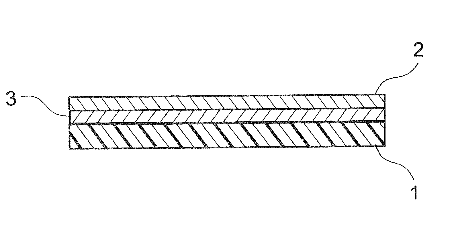
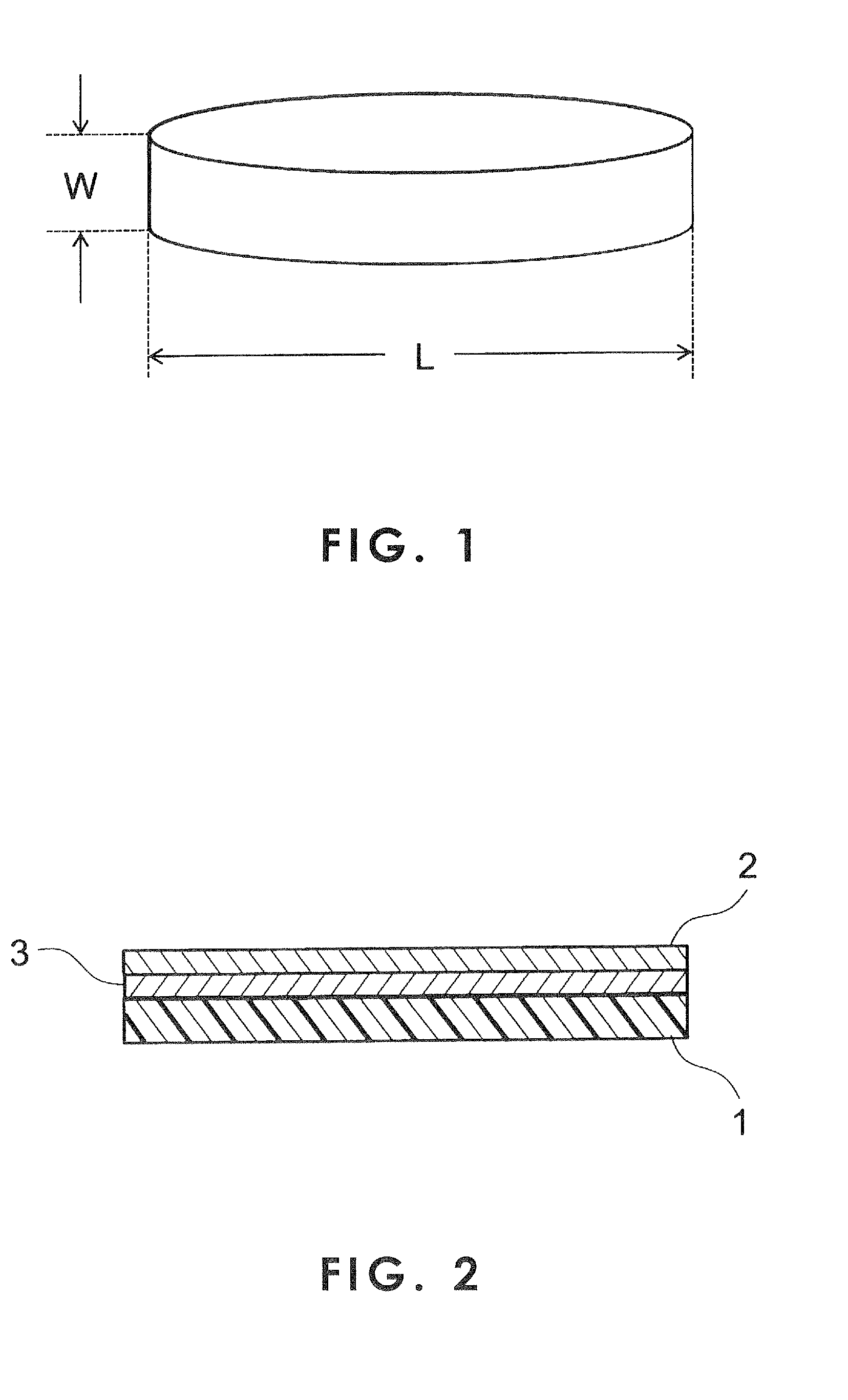
The present invention provides a polycrystalline aluminum nitride substrate that has a similar thermal expansion coefficient to GaN, making it ideal for growing GaN-based semiconductors. This substrate can help achieve a high yield of GaN-based semiconductor production. FIG. 1 shows a diagram of the polycrystalline aluminum nitride substrate, while FIG. 2 explains a method for manufacturing a GaN-based semiconductor using this substrate.

Problems solved by technology

These substrates, however, suffer from problems such as high cost (sapphire and SiC) and warpage due to a difference in linear expansion coefficient between gallium nitride and substrate materials.

Method used


Image

  • POLYCRYSTALLINE ALUMINUM NITRIDE BASE MATERIAL FOR CRYSTAL GROWTH OF GaN-BASE SEMICONDUCTOR AND METHOD FOR MANUFACTURING GaN-BASE SEMICONDUCTOR USING THE SAME
  • POLYCRYSTALLINE ALUMINUM NITRIDE BASE MATERIAL FOR CRYSTAL GROWTH OF GaN-BASE SEMICONDUCTOR AND METHOD FOR MANUFACTURING GaN-BASE SEMICONDUCTOR USING THE SAME

Examples


example 1

[0047]An aluminum nitride powder (mean particle diameter 1 μm, oxygen content 1.0% by weight) and a yttria (Y2O3) powder (mean particle diameter 1 μm), and an alumina (Al2O3) powder (mean particle diameter 1 μm) were mixed together at a mixing ratio specified in Table 1 to prepare a starting material powder. Regarding the mixing amounts in the table, yttria that is a first sintering aid, alumina that is a second sintering aid, and the aluminum nitride powder were mixed together to give a 100 parts by weight of the starting material powder.

[0048]After the mixing, the starting material powder was added to a solvent such as toluene or ethanol, and a dispersant was added thereto. Thereafter, an organic binder and a plasticizer were added followed by further mixing. The mixture was formed into a 1.2 mm-thick green sheet by doctor blading. The green sheet was cut into a size of 170 mm in length×170 mm in width, was then degreased, and was sintered under conditions of 1700° C.×5 hr to prep...

example 2

[0051]An experiment was carried out in the same manner as in Example 1, except that Gd2O3 (samples 9 to 14) was used as the first sintering aid and alumina was used as the second sintering aid. The aluminum nitride powder (impurity oxygen content 1.2% by weight), the first sintering aid, and the second sintering aid used each had a mean particle diameter of 1.2 μm. The sintering was carried out at a temperature in the range of 1700° C. to 1800° C. and, for all the sheets, the sintering was carried out in a nitrogen atmosphere. For the samples thus obtained, measurements were carried out in the same manner as in Example 1. The results are shown in Table 2.

TABLE 2Sample 9Sample 10Sample 11Sample 12Sample 13Sample 14Mixing amount of0.94.710.020.230.035.0Gd2O3 (pts. wt)Mixing amount of0.01.96.08.421.026.0Al2O3 (pts. wt)Volume fraction of97.692.185.680.058.548.6AlN phase insintered compactMean grain diameter9.76.94.83.42.52.3(μm)Constituent phaseMainlyMainlyMainlyMainlyMainlyMainlyother ...

example 3

[0053]An experiment was carried out in the same manner as in Example 1, except that Dy2O3 (samples 15 to 20) was used as the first sintering aid and alumina was used as the second sintering aid. The aluminum nitride powder (impurity oxygen content 1.2% by weight), the first sintering aid, and the second sintering aid used each had a mean particle diameter of 1.2 μm. The sintering was carried out at a temperature in the range of 1700° C. to 1800° C. and, for all the sheets, the sintering was carried out in a nitrogen atmosphere. For the samples thus obtained, measurements were carried out in the same manner as in Example 1. The results are shown in Table 3.

TABLE 3Sample 15Sample 16Sample 17Sample 18Sample 19Sample 20Mixing amount of0.94.710.022.030.035.0Gy2O3 (pts. wt)Mixing amount of0.01.94.68.915.016.0Al2O3 (pts. wt)Volume fraction of98.093.486.380.059.249.8AlN phase insintered compactMean grain diameter9.87.04.93.52.62.4(μm)Constituent phaseMainlyMainlyMainlyMainlyMainlyMainlyothe...


PUM

PropertyMeasurementUnit
Temperatureaaaaaaaaaa

Abstract

There is provided a polycrystalline aluminum nitride base material having a linear expansion coefficient similar to GaN. The polycrystalline aluminum nitride base material as a substrate material for crystal growth of GaN-base semiconductors has a mean linear expansion coefficient of 4.9×10⁻⁶ / K to 6.1×10⁻⁶ / K between 20° C. and 600° C. and 5.5×10⁻⁶ / K to 6.6×10⁻⁶ / K between 20° C. and 1100° C.

Description

TECHNICAL FIELD[0001]The present invention relates to a polycrystalline aluminum nitride base material for the growth of a GaN-base semiconductor crystal and a method for manufacturing a GaN-base semiconductor using the same.BACKGROUND ART[0002]The development of new light sources, for example, LEDs (light emitting diodes), photosemiconductor devices such as semiconductor lasers, and power devices using wide band gap semiconductors has been promoted from the viewpoints of environmental problems and energy saving.[0003]Regarding semiconductors for use in these devices, gallium nitride (GaN) base semiconductors such as GaN, InGaN, AlGaN, and InAlGaN have drawn attention and have been used as layers constituting the devices. For example, LED elements have a structure including a stack of a plurality of thin GaN-base layers. For example, Japanese Patent Laid-Open No. 111766 / 2004 (patent document 1) uses a multilayer structure of a GaN layer and a GaAlN layer. The yield of semiconductor ...

Claims


Application Information

Patent Timeline
IPC IPC(8): H01L21/02C04B35/581
CPCC04B35/581Y10T428/21C04B41/5062C04B41/87C04B2111/00844C04B2235/3217C04B2235/3222C04B2235/3224C04B2235/3225C04B2235/3852C04B2235/3886C04B2235/5436C04B2235/5445C04B2235/80C04B2235/9607C30B25/18C30B29/406H01L21/02389H01L21/0254C04B41/009C30B29/403C04B41/4531
Inventor MIYASHITA, KIMIYAKOMATSU, MICHIYASUAOKI, KATSUYUKIFUNAKI, KAI
Owner KK TOSHIBA
Learn More