Organic floating gate memory device having protein and method of fabricating the same

a floating gate memory and protein technology, applied in thermoelectric devices, solid-state devices, nano-informatics, etc., can solve the problems of substantial increase in production costs and process complexity, and achieve the effect of increasing the flexibility of the organic floating gate memory devi

Inactive Publication Date: 2013-07-18
NATIONAL TSING HUA UNIVERSITY
View PDF3 Cites 8 Cited by
  • Summary
  • Abstract
  • Description
  • Claims
  • Application Information

AI Technical Summary

Benefits of technology

[0013]In the organic floating gate memory device having protein of the present invention, the protein dielectric layer has a bioprotein which is modified or non-modified, and the bioprotein is a silk protein. The protein dielectric layer serves as the tunneling layer in the floating gate memory device, and carriers in the semiconductor layer may penetrate to the floating gate electrode under the effect of vertical electric field. After the vertical electric field is

Problems solved by technology

In addition, when a common dielectric material is to be formed for the gate dielectric or insulating layer in an organic floating gate memory de

Method used


Image

  • Organic floating gate memory device having protein and method of fabricating the same
  • Organic floating gate memory device having protein and method of fabricating the same
  • Organic floating gate memory device having protein and method of fabricating the same

Examples


example 1

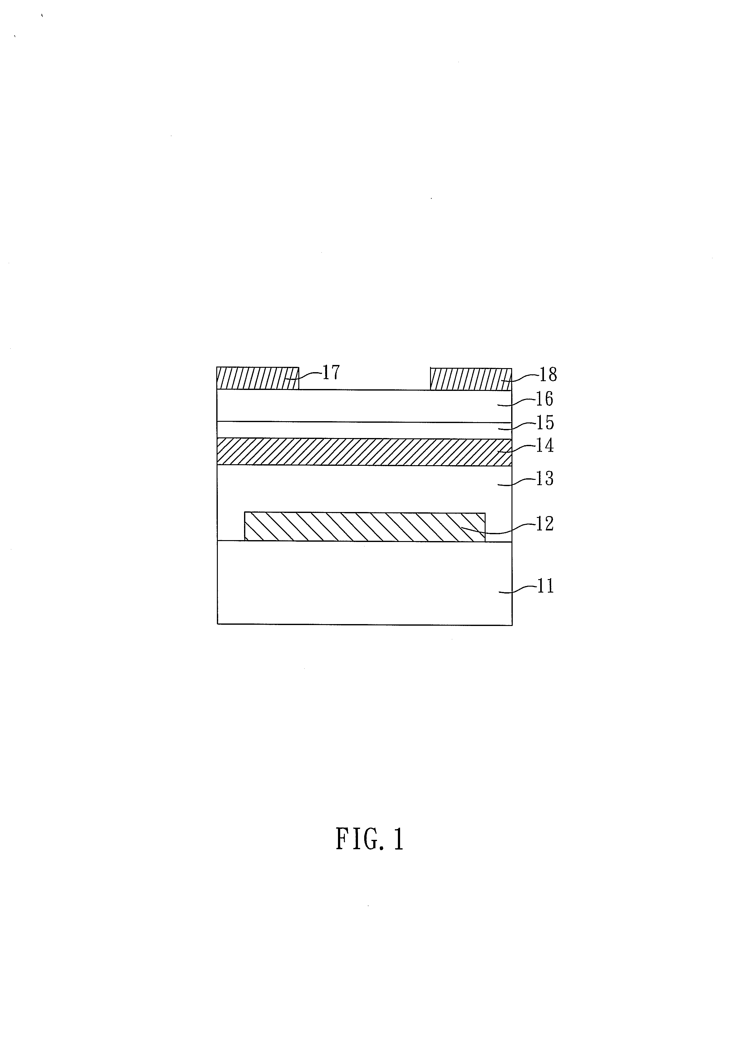
Top-Contact Organic Floating Gate Memory Device Having A Protein Material

Preparation of Silk Solution

[0038]First, an aqueous 10 wt % sodium carbonate solution is prepared and heated to boil. The solution is further boiled for 30 minutes to 1 hour to remove the sericin in the outer layer of silk after addition of dried silkworm cocoon (natural silk). Then, the silk is washed by deionized water to remove the alkaline solution on the outer layer of silk. After drying, a refined silk protein, namely, fibroin, is obtained.

[0039]Next, the refined silk protein is placed, stirred, and dissolved in a 20 ml of 85 wt % H3PO4 solution. After that, the H3PO4 solution containing dissolved silk protein is placed in a dialysis membrane (Spectra / Por 3 dialysis membrane, molecular weight cutoff=14000) and dialyzed with water for 3 days, to remove the excess phosphate. By controlling the water volume and the dialysis frequency, not only the phosphate can be removed, but also the pH value of the obtain...

example 2

Bottom-Contact Organic Floating Gate Memory Device Having A Protein Material

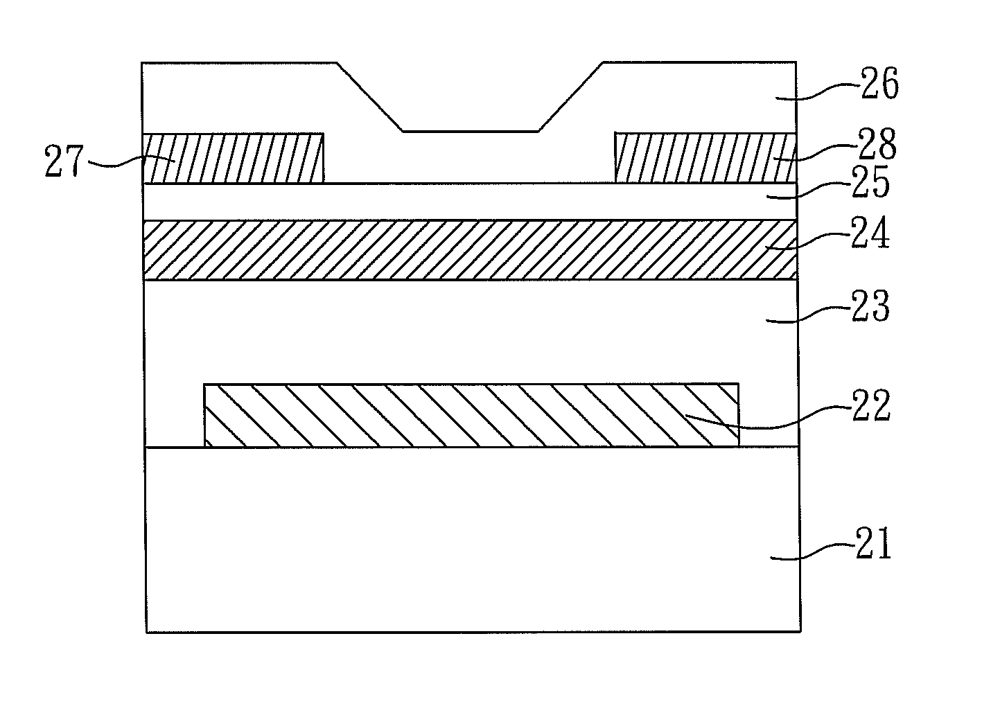
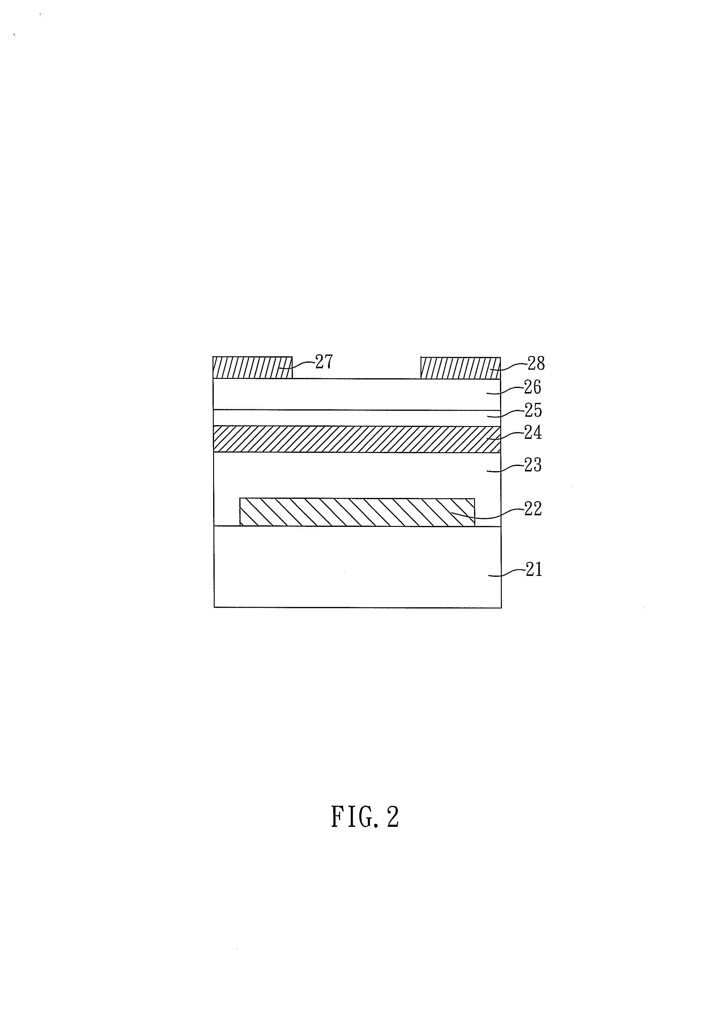
[0053]Referring to FIG. 4, a substrate 21 is provided, and gate electrode 22 and gate dielectric layer 23 are formed thereon sequentially. In this Example, the same method for manufacturing the substrate 21, gate electrode 22, and gate dielectric layer 23 as in Example 1 is performed. In this Example, the gate electrode has a thickness of 80 nm, and the gate dielectric layer 23 has a thickness of 400 nm.

[0054]Then, a mask (not shown) is used to form a patterned metal layer on the gate dielectric layer 23 by evaporation coating, to form a floating gate electrode 24 made of gold. By the same method as in Example 1, a biopolymer protein film is formed on the floating gate electrode 24 to serve as the protein dielectric layer 25.

[0055]Through the same process conditions for forming the gate electrode as in Example 1, a patterned metal layer is formed on the protein dielectric layer 25 by evaporation coating, to ...


PUM


Abstract

An organic floating gate memory device having protein and a method of fabricating the same are disclosed. The organic floating gate memory device of the present invention comprises: a substrate; a gate electrode on the substrate; a gate dielectric layer covering the gate electrode; a floating gate on the gate dielectric layer; a protein dielectric layer covering the floating gate; and an organic semiconductor layer, a source and a drain, wherein the organic semiconductor layer, the source and the drain are disposed over the protein dielectric layer

Description

BACKGROUND OF THE INVENTION[0001]1. Field of the Invention[0002]The present invention relates to an organic floating gate memory device having protein and a method of fabricating the same, and particularly to an organic floating gate memory device using protein as a dielectric layer and a method of fabricating the same.[0003]2. Description of Related Art[0004]With the rapid development of technology, electronic products such as mobile phones, notebook computers, tablet personal computers, flash drives, and digital cameras have become our daily necessity. Memory devices, which play an important role in these electronic products, can be generally classified into volatile memory and non-volatile memory. Volatile memory refers to that computer memory for which the storage data in it will disappear with the removal of the external power supply. Examples of volatile memory include static random access memory, and dynamic random access memory. Non-volatile memory refers to the kind for whi...

Claims


Application Information

Patent Timeline
IPC IPC(8): H01L51/30H01L51/40
CPCH01L51/0093H01L51/052B82Y10/00H01L51/0545H01L51/0554H01L51/0529H10K85/761H10K10/474H10K10/471H10K10/482H10K10/466
Inventor HWANG, JENN-CHANGTSAI, LI SHIUANGAN, JON-YIEW
Owner NATIONAL TSING HUA UNIVERSITY
Why Eureka
Try Eureka