Composite build-up material for embedding of circuitry

a technology of build-up material and circuitry, which is applied in the direction of dielectric characteristics, light absorption dielectrics, conductive pattern formation, etc., can solve the problems of high cte of rcf material, increase production time and therefore cost, and difficult to create, so as to reduce process steps, reduce voc content, and high dimensional stability

Inactive Publication Date: 2013-08-08
ATOTECH DEUT GMBH
View PDF9 Cites 10 Cited by
  • Summary
  • Abstract
  • Description
  • Claims
  • Application Information

AI Technical Summary

Benefits of technology

[0010]It is, therefore, an objective of the present invention to provide composite build-up materials for embedding of circuitry which avoid the disadvantages of RCF, RRCF and prepreg material currently used for embedding of circuitry. The objects of the present invention are to provide composite build-up materials having a low VOC content and a high dimensional stability. Furthermore, such composite build-up materials should be obtained by a manufacturing process with reduced process steps. In addition, the build-up material should not be brittle and easy to handle during manufacturing and in successive manufacturing steps. Vias and the like should be easily obtained by laser drilling and trenches by laser ablation.SUMMARY OF THE INVENTION
[0015]The resin layer without reinforcement is suitable for fine patterns formed by laser ablation techniques and is capable to host embedded circuitry and provide sufficient mechanical stability. Furthermore, manufacturing of printed circuit boards, IC substrates, chip packages with embedded circuitry using the inventive composite build-up materials needs less production steps when using the composite build-up materials. The composite build-up material has a high dimensional stability and has a low VOC content.

Problems solved by technology

On the other hand the CTE of the RCF material is rather high which is a severe disadvantage, e. g., in thermal cycling tests and solder dip tests (relevant test procedures: JESD22-A104-B, J-STD-003A).
On the other hand it is more difficult to create features such as microvias, trenches and pads through the glass fabric which significantly increases production times and therefore cost.
The handling of the sensitive prepregs is problematic, because the brittle prepreg material can chip away at the edges, for example during transport.
Another general disadvantage of prepreg materials is their VOC (volatile organic compounds) content because of the manufacturing process of the substrate materials which comprises one or more solvent-based wet chemical coating steps.
Furthermore, laser drilling of microvias and through holes as well as formation of trenches by laser ablation is more difficult due to the reinforcement embedded in prepreg materials.
In general the structuring of reinforced materials with laser is difficult.
Furthermore, light from a laser is reflected in a uncontrolled way by the reinforcement especially in case of the commonly used reinforcements made of glass.
This leads to an incomplete removal of build-up material.
The density of reinforcement in a resin layer is not homogeneous on a microscopic scale.
This leads to a non-uniform ablation by laser light, too.

Method used


Image

  • Composite build-up material for embedding of circuitry
  • Composite build-up material for embedding of circuitry
  • Composite build-up material for embedding of circuitry

Examples


example

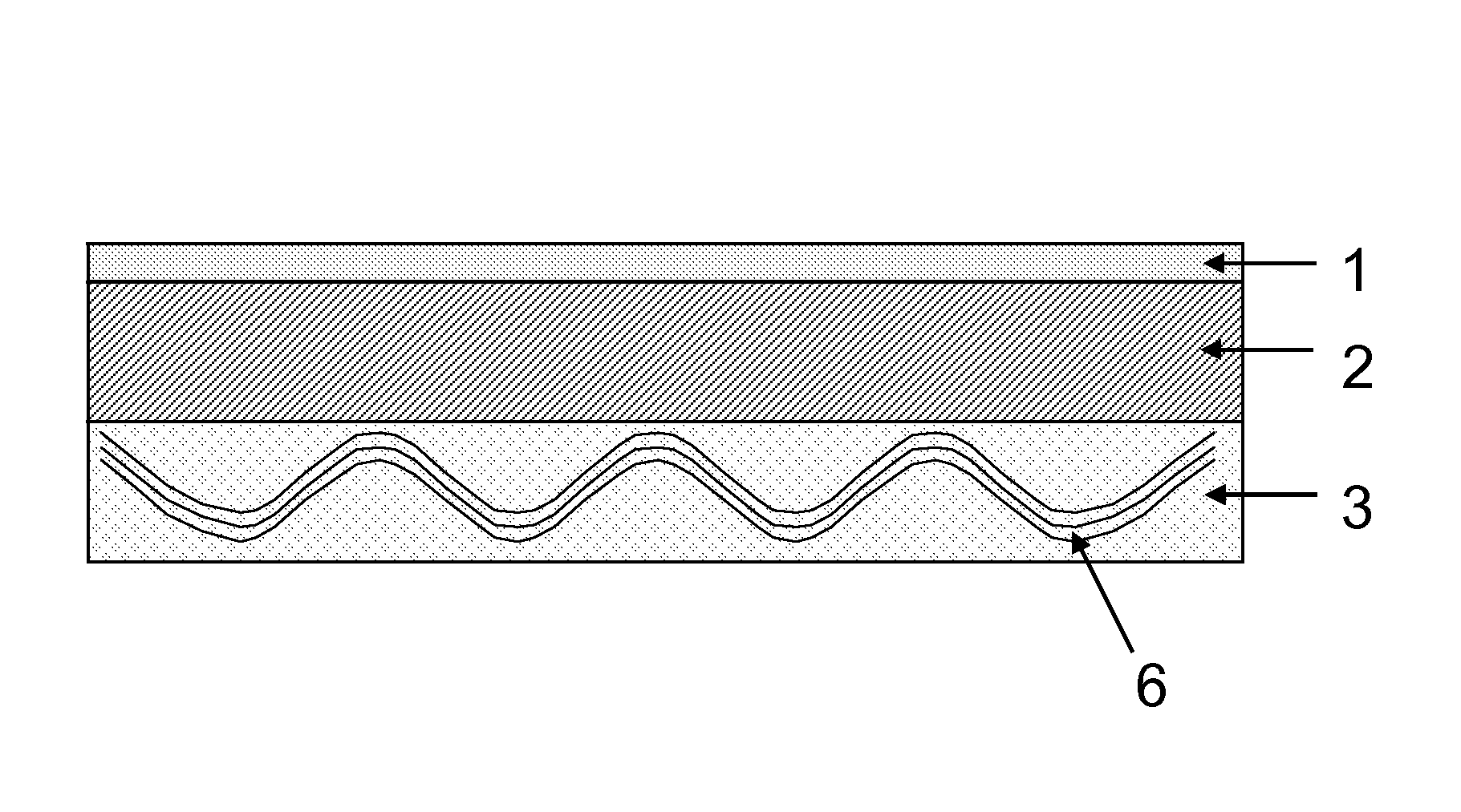
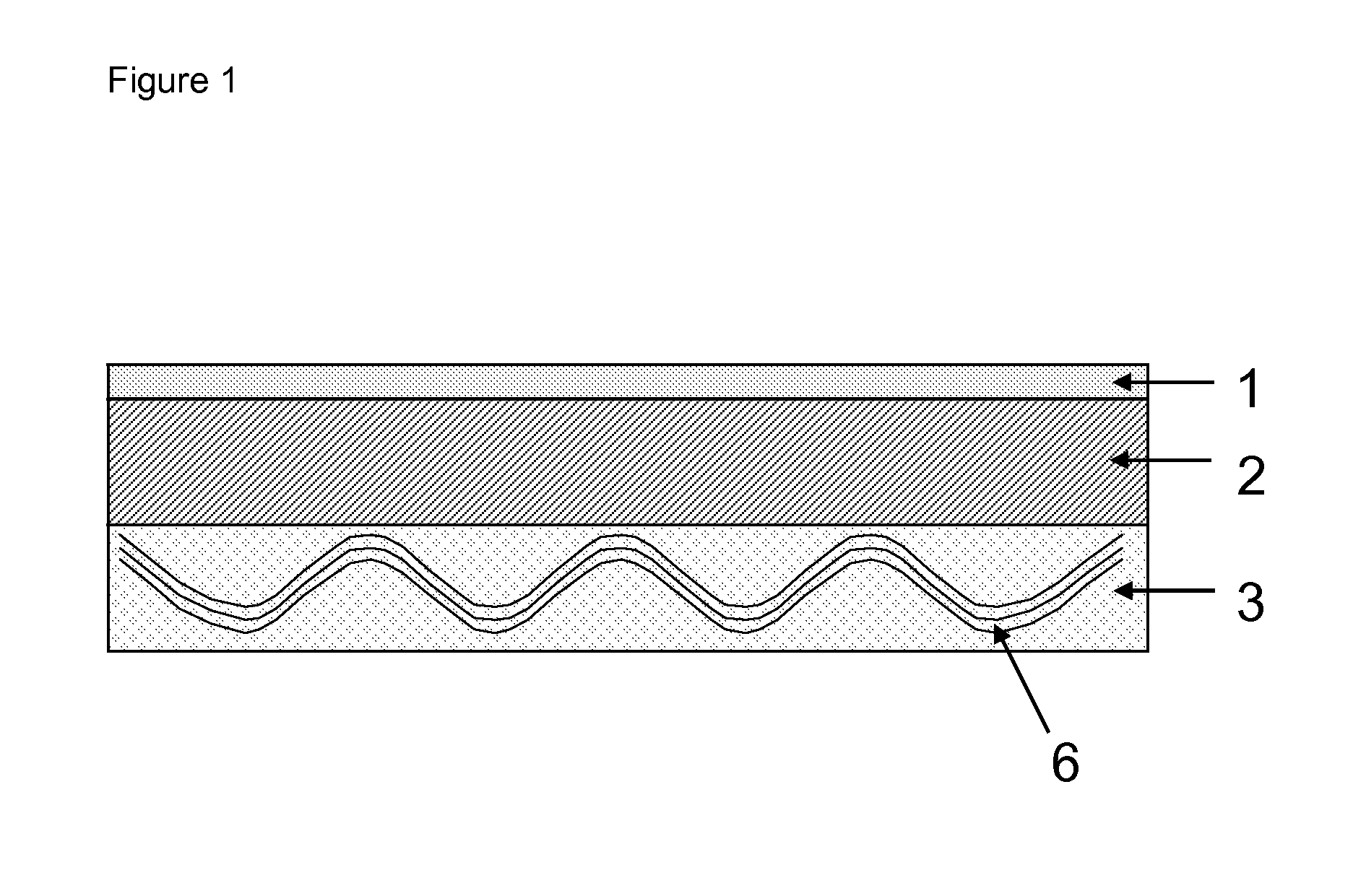
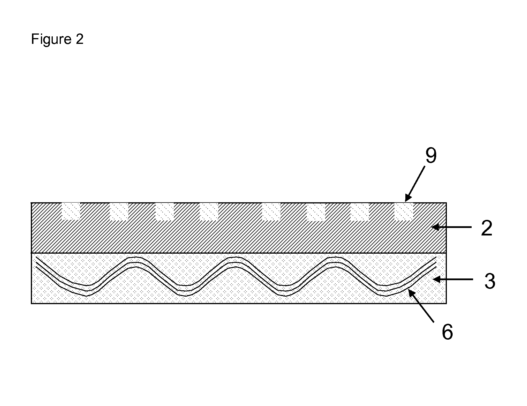
[0141]Preparation of Resin Powders for Layers (2) and (3)

[0142]The resin components listed in Table 1 were weighed out in the quantities shown and thoroughly mixed together in a polyethylene bag.

TABLE 1components used for the preparation of theresin powders for resin layers (2) and (3).ComponentQuantity (g)Multifunctional solid epoxy resin480Bakelit PF 0790 K03180Submicron sized silica338Total:998

[0143]A dicyclopentadienyl-bridged multifunctional solid epoxy resin, Bakelit PF 0790 K03 which is a phenol-formaldehyde-based, phenolic resin (CAS-no. 9003-35-4), and a submicron sized silica filler with an average particle size of 0.3 microns and a spherical particle shape, are used as raw materials. The mixed components of the dielectric were then extruded on a 19 mm-bore, 5-zone, 24 l / d, twin screw extruder made by OMC, Italy and fitted with screws having the maximum number of mixing elements. The barrel temperature in the mixing zones was set to 100° C. and the rotation speed to 600 rp...


PUM

PropertyMeasurementUnit
thicknessaaaaaaaaaa
thicknessaaaaaaaaaa
temperaturesaaaaaaaaaa

Abstract

Disclosed are composite build-up materials for the manufacture of printed circuit boards, IC substrates, chip packages and the like. The composite build-up materials are suitable for embedding circuitry such as microvias, trenches and pads. The composite build-up materials comprise a carrier layer (1), a resin layer without reinforcement (2), and a resin layer with reinforcement (3). The circuitry (9) is embedded into the resin layer without reinforcement (2).

Description

FIELD OF THE DISCLOSURE[0001]The invention relates to build-up materials for manufacture of printed circuit boards, IC substrates, chip packages and the like, suitable for embedding circuitry to form electrical paths for signal propagation.BACKGROUND OF THE INVENTION[0002]Circuitry such as copper tracks (such as copper filled microvias, trenches and pads) are mounted on one or both outer surfaces of substrate materials which are then stacked and laminated to form devices such as printed circuit boards, IC substrates, chip packages and the like. Due to the ongoing demand for size reduction of such devices, circuitry features such as width of copper tracks and the space between two copper tracks have to be reduced further. To achieve this goal conventional methods for manufacture of copper tracks such as roughening the surface of the non-conductive substrate followed by copper deposition onto the substrate surface and print and etch procedures need to be replaced by more fine-line cap...

Claims


Application Information

Patent Timeline
Patent Type & Authority Applications(United States)
IPC IPC(8): H05K3/00H05K1/03
CPCH05K2201/0112H05K2201/0195H05K2201/029H05K2201/0293Y10T428/24967H05K3/4673H05K1/0313H05K3/0085Y10T29/49155H05K3/0032H05K3/10H05K3/46
Inventor BRUDERER, ALEXGALSTER, NORBERTKRESS, JURGENPROBST, MICHEL
Owner ATOTECH DEUT GMBH
Why Eureka
Try Eureka