Vertical junction solar cell structure and method

Inactive Publication Date: 2013-08-29
SHARP KK
View PDF1 Cites 29 Cited by
  • Summary
  • Abstract
  • Description
  • Claims
  • Application Information

AI Technical Summary

Benefits of technology

[0032]More specifically, the present invention exploits the combination of efficient light trapping and uniform carrier generation that can be achieved in non-close packed arrangement to achieve the technical effects of maximizing both the short circuit current density Jsc and open circuit voltage Voc of the cell. For example, the reflectivity of a cell in accordance with the present invention depends on the average pitch of the nanostructures and may include one or more minima. In addition

Problems solved by technology

Balancing of these factors compromises the efficiency of the solar cell.
These competing optical and electronic length scales mean that the efficiency of the solar cell is compromised by selection of an active layer thickness that is compatible with both absorption and extraction.
However, a number of practical constraints mean that it is challenging to fully exploit their potential.
Fabrication of close-packed nanostructured solar cells by disposing thin films over a h

Method used


Image

  • Vertical junction solar cell structure and method
  • Vertical junction solar cell structure and method
  • Vertical junction solar cell structure and method

Examples


Example

First Embodiment

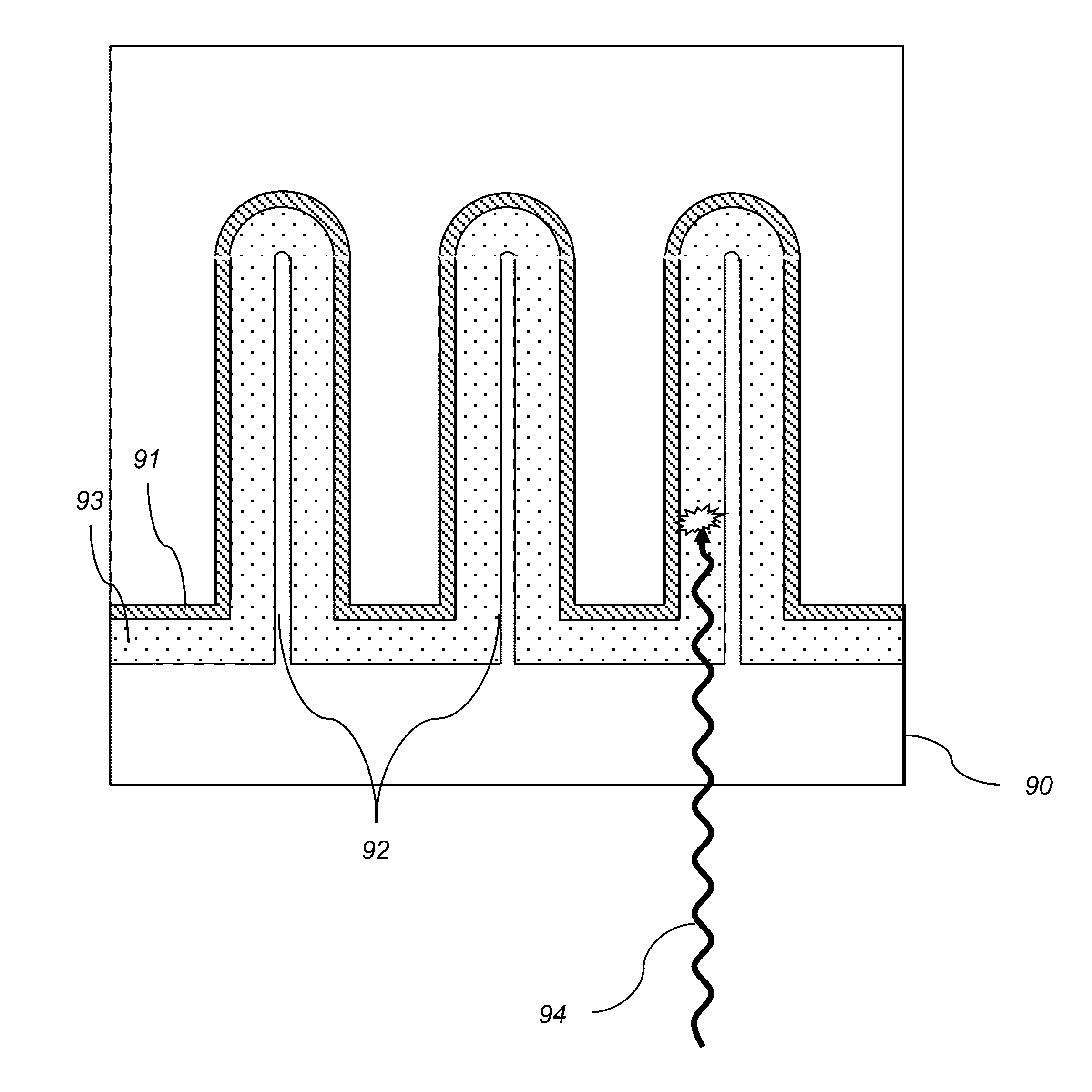
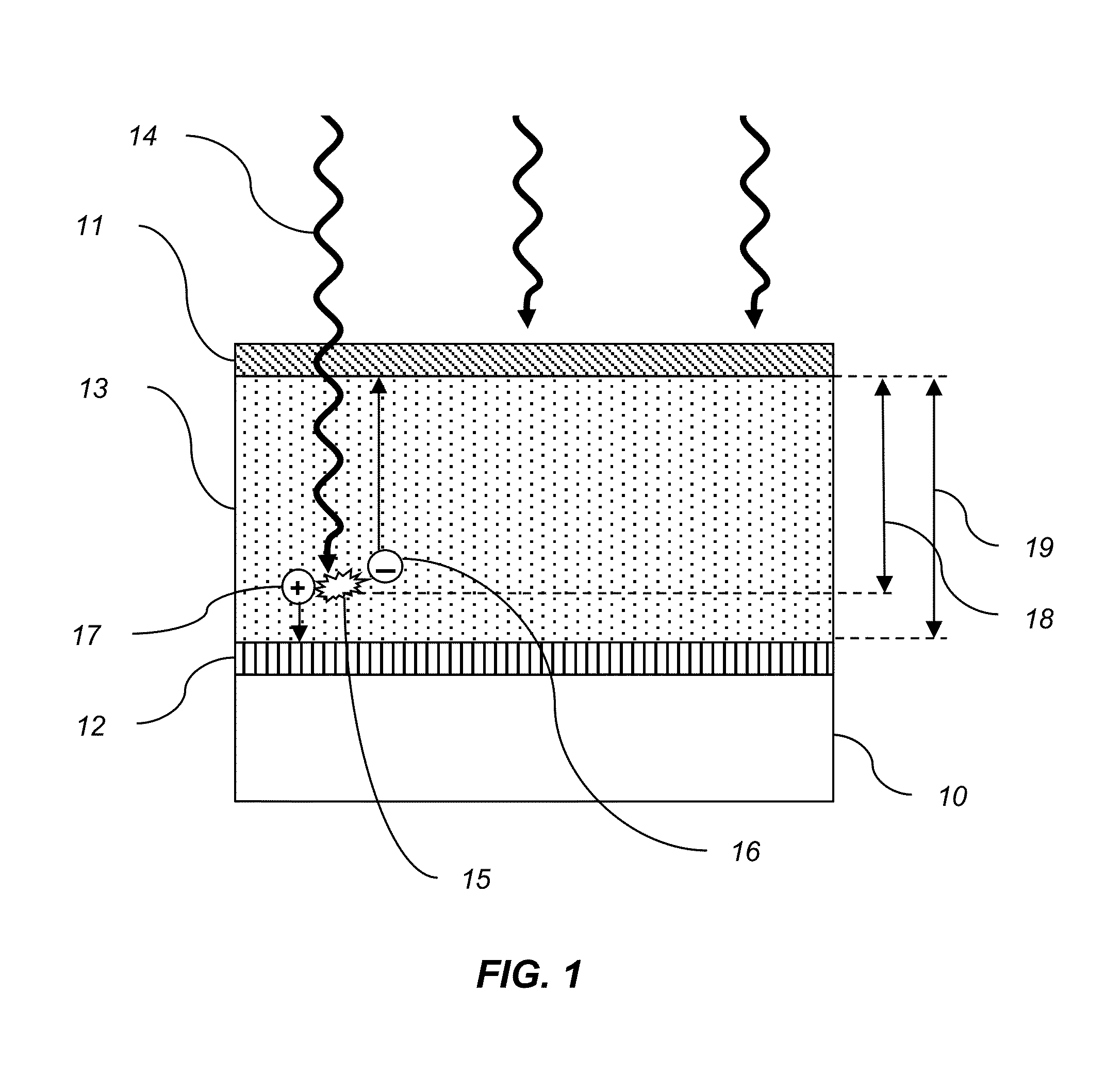
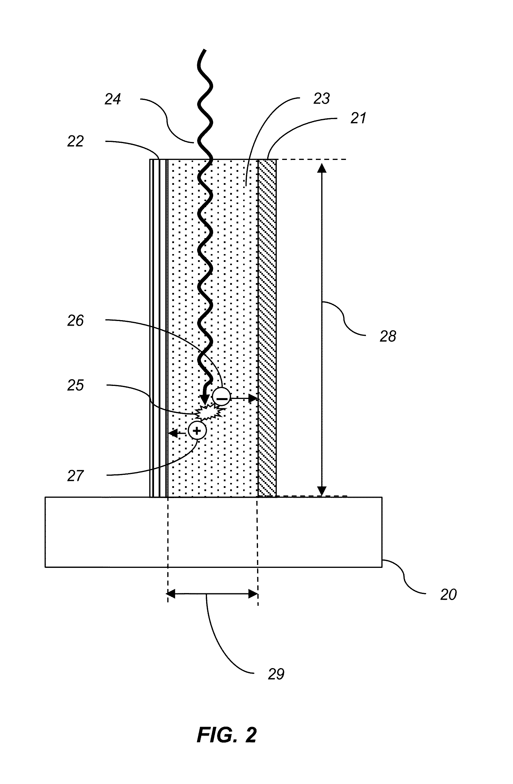
[0192]In a first embodiment of the present invention, shown in FIG. 5 in both an elevation and a plan view, a vertical junction nanostructured thin film solar cell includes a substrate 50 upon which there is formed a two dimensional array of elongate nanostructures 52 extending substantially vertically from a top surface of the substrate. The elongate nanostructures may be formed as a separate layer or component, or the elongate nanostructures may be fashioned integrally with or from the substrate itself. For example, the elongate nanostructures may be fashioned by removing material from the top surface of the substrate. In such case the nanostructures can be considered to be integral to the substrate rather than distinct features formed on or added to the substrate.

[0193]The solar cell structure further includes a thin film solar cell disposed over the elongate nanostructures such that the thin film solar cell substantially conforms to the topography of the nanostru...

Example

Second Embodiment

[0211]In a second embodiment, a vertical junction nanostructured thin film solar cell may be formed by a process of: 1) forming a substrate, 2) forming a two dimensional array of elongate nanostructures extending substantially perpendicularly from a surface of the substrate; and 3) disposing a thin film solar cell over the nanostructures such that the thin film substantially conforms to the topography of the nanostructures using a process that may be of any suitable type including, hydrogenated amorphous silicon (a-Si:H), microcrystalline silicon (uc-Si), cadmium telluride (CdTe), copper indium gallium sellenide or sulfide (CIGS), organic or polymer materials, or colloidal quantum dots.

Example

Third Embodiment

[0212]In a third embodiment, the elongate nanostructures are formed on a substrate by, in one case, an additive method such as a one-dimensional growth method, for example, metal catalysed vapor-liquid-solid (VLS) growth, or solid-liquid-solid (SLS) growth. In another variation, the elongate nanostructures are formed by a subtractive method such as masking and etching of the substrate. In yet another variation, the elongate nanostructures are formed by a combination of an additive and subtractive methods such as layer deposition followed by masking and etching of the layer.


PUM


Abstract

A non-close-packed vertical junction photovoltaic device includes a substrate, a two-dimensional array of elongate nanostructures extending substantially perpendicularly from a surface of the substrate, and a thin film solar cell disposed over the nanostructures such that the thin film solar cell substantially conforms to the topography of the nanostructures. An average separation of nearest neighbor solar cell coated nanostructures is greater than zero and less than a vacuum wavelength of light corresponding to a band gap of absorption. The thin film solar cell may include an active region that conforms to the elongate nanostructures, a first electrode that conforms to a surface of the active region, and a second electrode. A separation of opposing outer surfaces of the first electrode extending along adjacent elongate nanostructures is greater than zero and less than the vacuum wavelength of the light corresponding to the band gap of the active region.

Description

TECHNICAL FIELD[0001]This invention relates to solar cells and, more particularly, to a device structure and method of making and incorporating a vertical junction for achieving higher efficiency in a solar cell.BACKGROUND ART[0002]A solar cell typically includes two contact electrodes and at least one active region including a semiconductor junction that provides photovoltaic action. For example, the semiconductor junction(s) may include a Schottky junction, a p-n junction, or a p-i-n junction. Free charge carriers generated by the absorption of photons in the active region are transported under the influence of an internal potential gradient provided by the junction to the contacts where they are collected and used to power an external circuit. For a solar cell to operate efficiently, at least the following is desired:[0003]1. The absorber material in the active region(s) should absorb as many incident photons as possible resulting in the generation of pairs of oppositely charged ...

Claims


Application Information

Patent Timeline
IPC IPC(8): H01L31/0352H01L31/18B82Y99/00
CPCH01L31/035281H01L31/075Y02E10/548B82Y30/00H01L31/202Y02P70/50
Inventor DAY, STEPHENDIMMOCK, JAMES ANDREW ROBERTKAUER, MATTHIAS
Owner SHARP KK
Why Eureka
Try Eureka