Semiconductor element having high breakdown voltage

a technology of semiconductor elements and breakdown voltages, applied in semiconductor devices, diodes, electrical devices, etc., can solve the problems of unsatisfactory reverse leakage current and breakdown voltage, and the overall manufacturing process is still complicated, so as to reduce leakage current and increase breakdown voltage

Inactive Publication Date: 2013-09-19
NAT CENT UNIV
View PDF0 Cites 7 Cited by
  • Summary
  • Abstract
  • Description
  • Claims
  • Application Information

AI Technical Summary

Benefits of technology

[0006]Therefore the primary object of the present invention is to solve the aforesaid disadvantages of unsatisfactory current leakage and breakdown voltage of a conventional Schottky diode and transistor element. Another object of the present invention is to overcome the issues of the additional fabricating processes for a guard ring and a heavily-doped region that are required for reducing a leakage current and increasing a breakdown voltage in conventional Schottky diode and transistor element.

Problems solved by technology

However, a Schottky diode and a transistor element manufactured from gallium nitride (GaN) usually suffer from unsatisfactory reverse leakage current and breakdown voltage.
Yet, on top of an additional masking process required for fabricating the guard ring, the guard ring also occupies an extra space such that a Schottky diode provided with a guard ring needs a larger space that disfavors a common goal of element miniaturization.
Although the above Schottky diode does not need the design of a guard ring and is capable of reducing a leakage current as well as increasing a breakdown voltage of the Schottky diode, an overall manufacturing process is nevertheless made complicated due to the additional doping process for fabricating the heavily-doped region.

Method used


Image

  • Semiconductor element having high breakdown voltage
  • Semiconductor element having high breakdown voltage
  • Semiconductor element having high breakdown voltage

Examples


Embodiment Construction

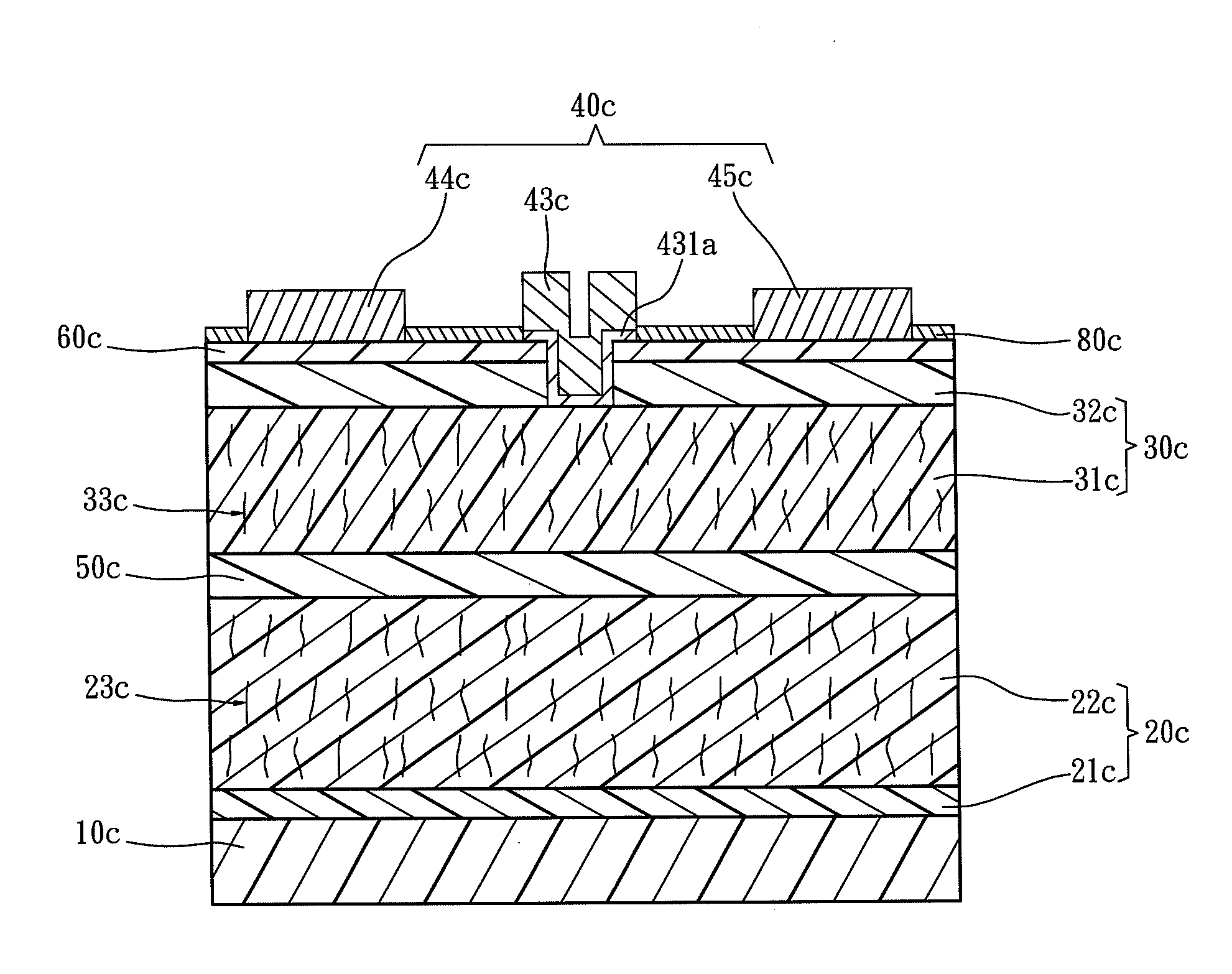
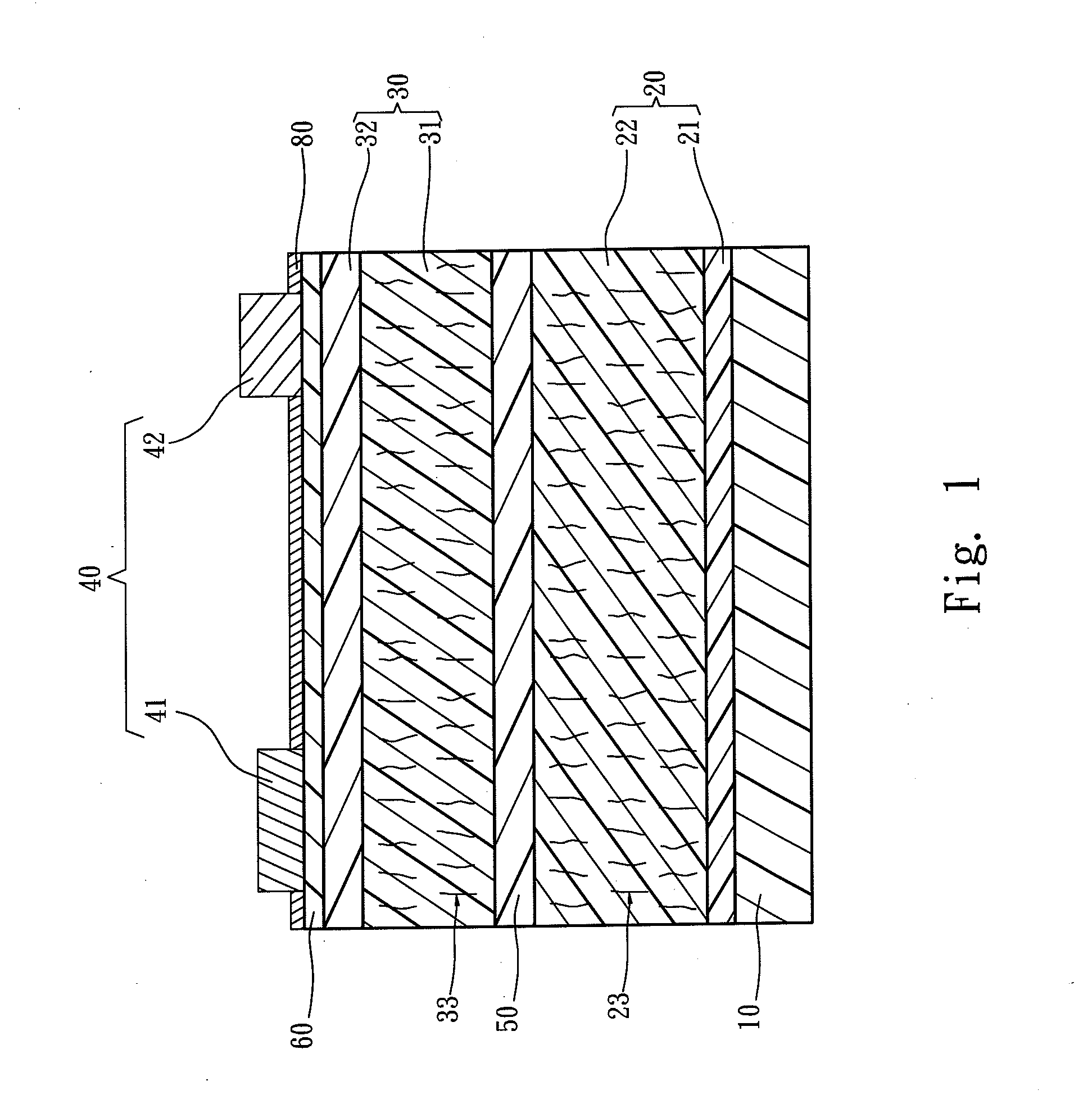
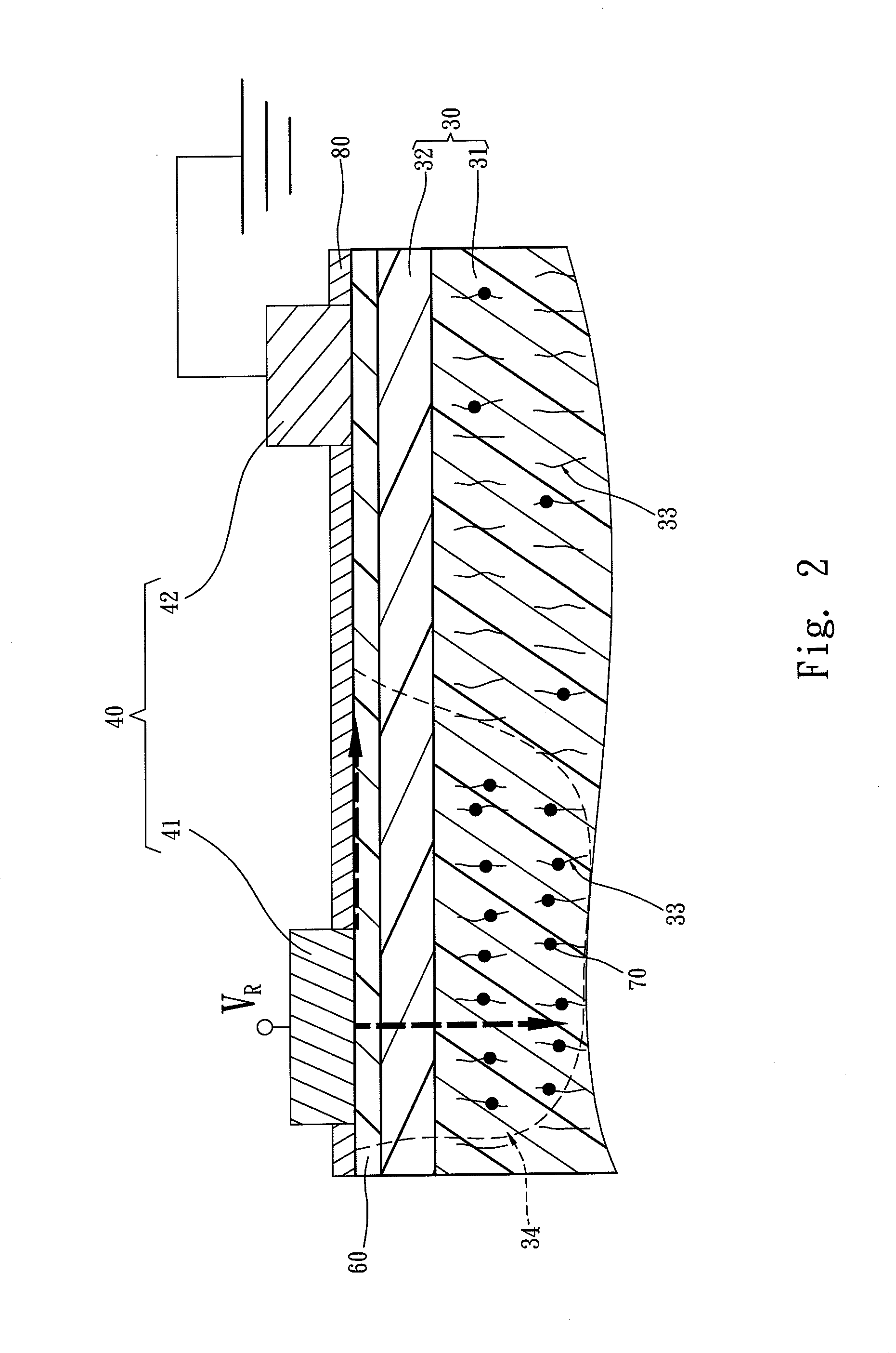
[0017]FIG. 1 shows a sectional view of a semiconductor element having a high breakdown voltage according to a first embodiment of the present invention. In this embodiment, for example, the semiconductor element is a Schottky diode. The semiconductor element comprises a substrate 10, a buffer layer 20, a semiconductor composite layer 30 and a bias electrode 40. The substrate 10 is a sapphire substrate. The buffer layer 20, disposed on the substrate 10, comprises an aluminum nitride (AlN) nucleation layer 21 and an AlN buffer layer 22 located on the AlN nucleation layer 21. The AlN buffer layer 22 comprises a first high edge dislocation defect density area. A common dislocation defect includes an edge dislocation defect, a spiral dislocation defect or a mixed dislocation defect. However, it should be noted that the first high edge dislocation defect density area according to the embodiment of the present invention means that the AlN buffer layer 22 has a larger number of edge disloca...


PUM


Abstract

A semiconductor element having a high breakdown voltage includes a substrate, a buffer layer, a semiconductor composite layer and a bias electrode. The buffer layer disposed on the substrate includes a high edge dislocation defect density area. The semiconductor composite layer disposed on the buffer layer includes a second high edge dislocation defect density area formed due to the first high edge dislocation defect density area. The bias electrode is disposed on the semiconductor composite layer. A virtual gate effect of defect energy level capturing electrons is generated due to the first and second high edge dislocation defect density areas, such that an extended depletion region expanded from the bias electrode is formed at the semiconductor composite layer. When the bias electrode receives a reverse bias, the extended depletion region reduces a leakage current and increases the breakdown voltage of the semiconductor element.

Description

FIELD OF THE INVENTION[0001]The present invention relates to a semiconductor element, and particularly to a semiconductor element having a high breakdown voltage.BACKGROUND OF THE INVENTION[0002]A power electronics including a transistor and a Schottky diode is frequently operated under high-power and high-temperature environments. Hence, III-nitrides having a high electric field and a large bandgap are often selected as an optimal choice for manufacturing a high-voltage and high-power power electronics including a transistor and a Schottky diode. Such power rectifier is applicable to high-power electronic elements including power distribution modules, power conditioning in large industrial motors, hybrid electric vehicles and switchers.[0003]However, a Schottky diode and a transistor element manufactured from gallium nitride (GaN) usually suffer from unsatisfactory reverse leakage current and breakdown voltage. To achieve a low leakage and a high breakdown voltage, a solution of ad...

Claims


Application Information

Patent Timeline
Patent Type & Authority Applications(United States)
IPC IPC(8): H01L29/205
CPCH01L29/4236H01L29/475H01L29/2003H01L29/7787H01L29/872H01L29/66212
Inventor CHYI, JEN-INNLEE, GENG-YENLIU, HSUEH-HSING
Owner NAT CENT UNIV
Why Eureka
Try Eureka