Switching power supply device

a power supply device and power supply technology, applied in the direction of electric variable regulation, process and machine control, instruments, etc., can solve the problems of power conversion efficiency reduction, difficulty in increasing the degree of magnetic coupling of the transformer, and the inability to control output. the effect of small power loss

Active Publication Date: 2013-11-14
MURATA MFG CO LTD
View PDF5 Cites 37 Cited by
  • Summary
  • Abstract
  • Description
  • Claims
  • Application Information

AI Technical Summary

Benefits of technology

[0009]Preferred embodiments of the present invention provide a switching power supply device with reduced size and increased power conversion efficiency.
[0025]According to various preferred embodiments of the present invention, an LC resonant circuit is disposed on each of the primary side and secondary side. The two LC resonant circuits are caused to resonate with each other, so that power transmission can be performed by utilizing magnetic field and electric field coupling between the primary winding and the secondary winding. In addition, with the resonance phenomenon allows only the real power to be transmitted from the primary side to the secondary side while the reactive power circulates in the LC resonant circuits on both the primary side and the secondary side, resulting in very small power loss. Furthermore, as to the switching frequency, switching elements in an overall multi-resonant circuit in which a primary-side resonant circuit and a secondary-side resonant circuit, which include an electromagnetic field coupling circuit, are combined are turned on and off at a frequency higher than a specific resonant frequency thereof at which the input impedance becomes minimum, thus enabling the switching element to perform a zero voltage switching (ZVS) operation.

Problems solved by technology

However, the degree of magnetic coupling of the transformer may be difficult to increase because magnetic saturation is prevented or because of physical constraints, resulting in power conversion efficiency being reduced.
In addition, in view of operation on the order of MHz for miniaturization of magnetic components, changes in operating frequency result in a significant problem in terms of the controllability of output, EMC (electromagnetic compatibility), and so forth.

Method used


Image

  • Switching power supply device
  • Switching power supply device
  • Switching power supply device

Examples


first preferred embodiment

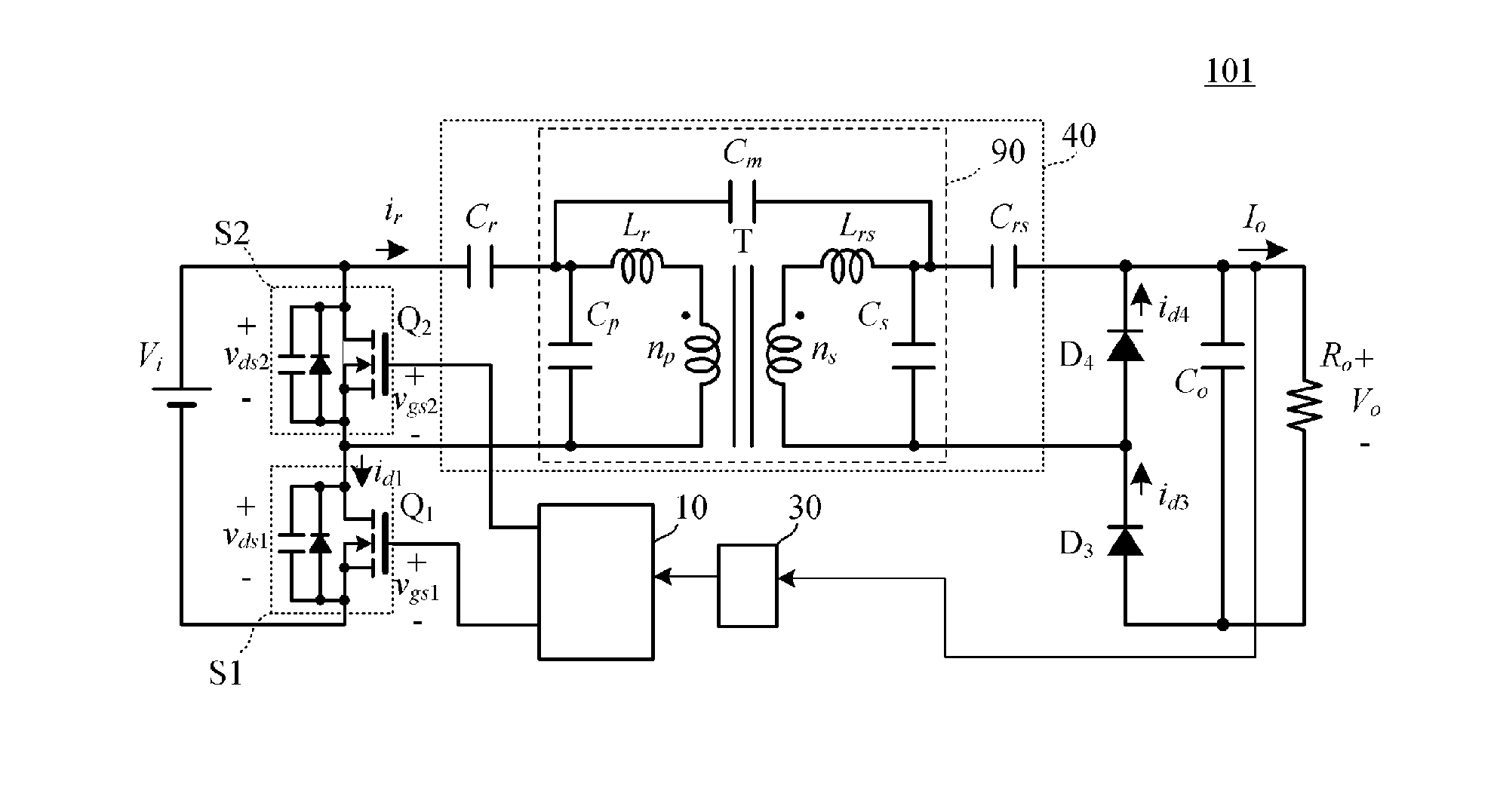
[0050]FIG. 2 is a circuit diagram of a switching power supply device 101 according to a first preferred embodiment of the present invention.

[0051]The switching power supply device 101 is a circuit including an input unit to which an input power supply Vi is input, and an output unit from which stable direct-current power is supplied to a load Ro. The switching power supply device 101 includes the units described below.

[0052]An electromagnetic field coupling circuit 90 includes a transformer including a primary winding np and a secondary winding ns.

[0053]A switching circuit S1 including a switching element Q1, and a switching circuit S2 including a switching element Q2, which are connected to the primary winding np, are also provided.

[0054]Rectifier diodes D3 and D4 and a smoothing capacitor Co, which are connected to the secondary winding ns, are provided.

[0055]A first LC series resonant circuit is connected to the primary winding np and defined by a series resonant inductor Lr and ...

second preferred embodiment

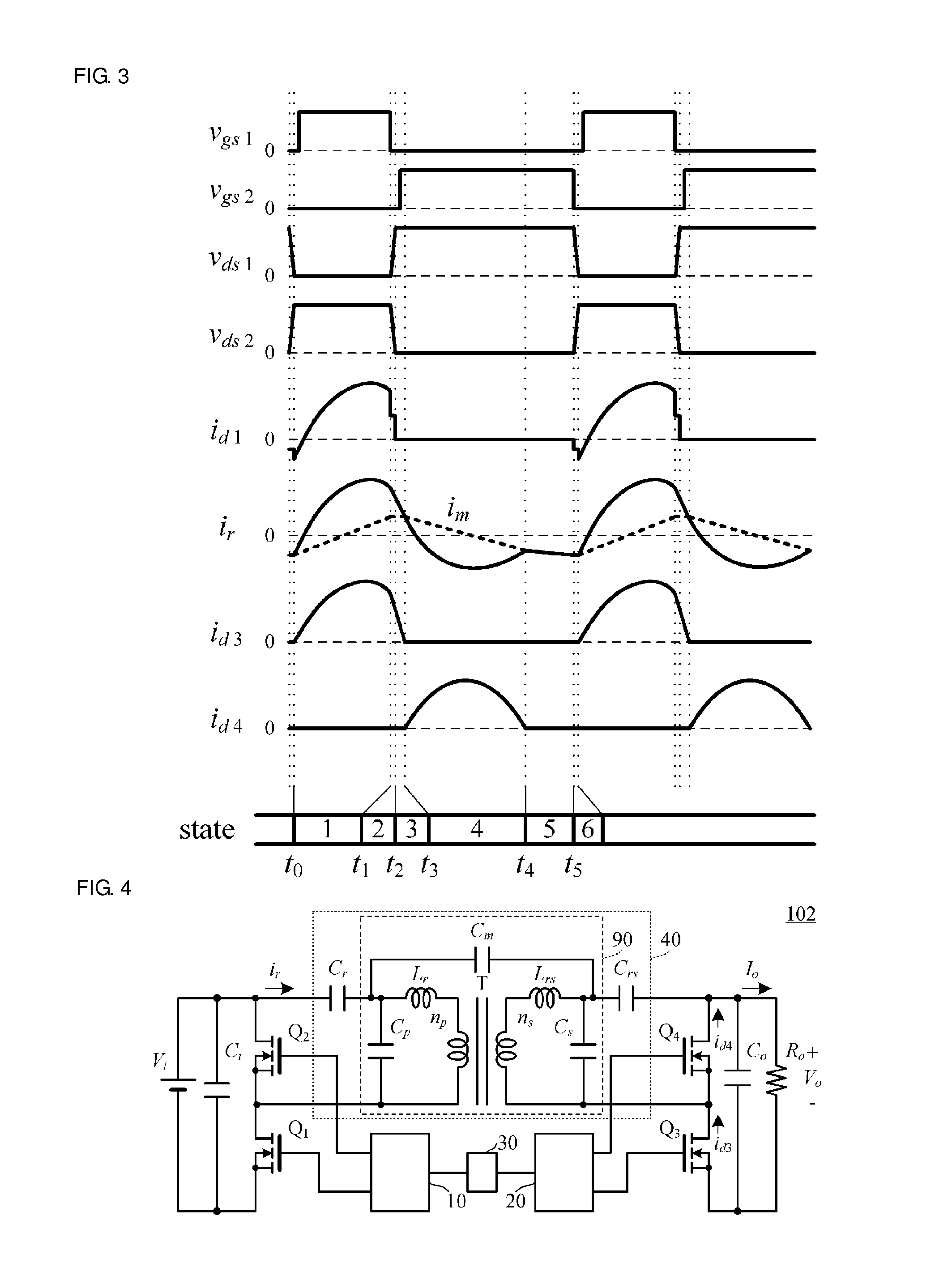
[0098]FIG. 4 is a circuit diagram of a switching power supply device 102 according to a second preferred embodiment of the present invention. In this example, unlike the switching power supply device 101 according to the first preferred embodiment, FET-type switching elements Q3 and Q4 are preferably disposed instead of the rectifier diodes D3 and D4 on the secondary side. That is, the switching elements Q3 and Q4 define a secondary-side rectifier circuit. The switching elements Q3 and Q4 each include a diode (parasitic diode) and a capacitor (parasitic capacitance) in parallel, and constitute switching circuits S3 and S4, respectively. In addition, a capacitor Ci is disposed in a power supply input unit. A switching control circuit 20 controls the switching elements Q3 and Q4 on the secondary side.

[0099]The magnetizing inductances Lm and Lms of the primary winding np and the secondary winding ns of the transformer T, and the parasitic capacitances and parasitic diodes of the switch...

third preferred embodiment

[0108]FIG. 6 is a circuit diagram of a switching power supply device 103 according to a third preferred embodiment. In this example, capacitors Ci1 and Ci2 that divide the voltage at the input power supply Vi, and capacitors Cis1 and Cis2 that divide the output voltage Vo are provided. Here, the inductors Lm and Lms, which are the magnetizing inductances of the primary winding np and the secondary winding ns of the transformer T or external inductances, are illustrated. The other components are similar to those in the second preferred embodiment illustrated in FIG. 4.

[0109]In the third preferred embodiment, the input voltage Vi is divided by the capacitors Ci1 and Ci2, and the output voltage Vo is divided by the capacitors Cis1 and Cis2. Since the capacitors Ci1 and Cis1 divide a direct-current input voltage, the capacitors Ci1 and Cis1 serve to hold a direct-current voltage. Thus, the series resonant capacitors Cr and Crs operate as capacitors for resonance, and do not serve to hol...


PUM


Abstract

In a switching power supply device with reduced size and increased power conversion efficiency, a first resonant circuit including a series resonant inductor and a series resonant capacitor, and a second resonant circuit including a series resonant inductor and a series resonant capacitor, are caused to resonate with each other to cause sympathetic vibration of each resonant circuit, such that transmission is performed by utilizing both magnetic field coupling and electric field coupling between a primary winding and a secondary winding. Operation at a switching frequency higher than a specific resonant frequency of an overall multi-resonant circuit allows a ZVS operation to be performed, enabling a significant reduction in switching loss and high-efficiency operation.

Description

BACKGROUND OF THE INVENTION[0001]1. Field of the Invention[0002]The present invention relates to a switching power supply device that includes a switching element on a primary side and a rectifier circuit on a secondary side and that performs power transmission by using the electromagnetic field resonance phenomenon.[0003]2. Description of the Related Art[0004]With recent progress toward compact and lightweight electronic devices, market demand for high-efficiency, compact, and lightweight switching power supplies has increasingly grown. For example, current resonant half-bridge converters that cause a transformer to operate in response to a sinusoidal resonant current flowing therethrough by using an LC resonance phenomenon have been increasingly put into practical use in markets of goods such as flat-screen televisions with comparatively moderated output current ripple characteristics, while taking advantage of the feature of high efficiency.[0005]For example, an LC series resonan...

Claims


Application Information

Patent Timeline
Patent Type & Authority Applications(United States)
IPC IPC(8): H02M3/335
CPCH02M3/33507H02M3/3381H02M3/33576Y02B70/10H02M1/0058H02M3/28H02M3/335H02M3/22H03K3/30
Inventor HOSOTANI, TATSUYA
Owner MURATA MFG CO LTD
Why Eureka
Try Eureka