Bipolar punch-through semiconductor device and method for manufacturing such a semiconductor device

a semiconductor device and bipolar technology, applied in the field of power electronics, can solve the problems of device non-uniform current, difficult to accurately cut the wafer, and thick buffer layer, and achieve the effect of reducing the concentration of doping

Active Publication Date: 2014-02-06
HITACHI ENERGY SWITZERLAND AG
View PDF1 Cites 7 Cited by
  • Summary
  • Abstract
  • Description
  • Claims
  • Application Information

AI Technical Summary

Benefits of technology

[0007]The method applied in EP 0 749 166 A1 can be complicated, time consuming and expensive due to the necessity of growing a plurality of epitaxial layers and even more complicated due to the growing the subsequent epitaxial layers with decreasing doping concentration and ending in a device with a thick buffer layer due to a thick highly doped wafer being used as a basis for the manufacturing.

Problems solved by technology

However, as the n layer from which the buffer layer is made, has to be cut within the rising doping profile as shown by the dashed line in FIG. 2, it is difficult to cut the wafer accurately.
However, a thicker buffer layer creates higher losses and variations in bipolar gain.
Furthermore, the device has non-uniform current.
It would be difficult if such devices were manufactured directly on a thin wafer, because working directly on thin wafers can be a rather complex process, if the wafer is thin in low voltage IGBTs for forming the frontside layers including the emitter MOS cells and termination and the backside layers including the anode and buffer regions.
However, even with the implementation of the described method above, such devices need optimization for improved static and dynamic performance with a number of limiting process options.
In addition, the larger the wafer diameter, the more the difficulties encountered for thin wafer processing.
Finally, the quality and availability of silicon substrate material is also an issue for thin wafer technologies utilizing for example deep diffused methods, for example, for larger wafer diameters above 200 mm.
The method applied in EP 0 749 166 A1 can be complicated, time consuming and expensive due to the necessity of growing a plurality of epitaxial layers and even more complicated due to the growing the subsequent epitaxial layers with decreasing doping concentration and ending in a device with a thick buffer layer due to a thick highly doped wafer being used as a basis for the manufacturing.

Method used


Image

  • Bipolar punch-through semiconductor device and method for manufacturing such a semiconductor device
  • Bipolar punch-through semiconductor device and method for manufacturing such a semiconductor device
  • Bipolar punch-through semiconductor device and method for manufacturing such a semiconductor device

Examples


Embodiment Construction

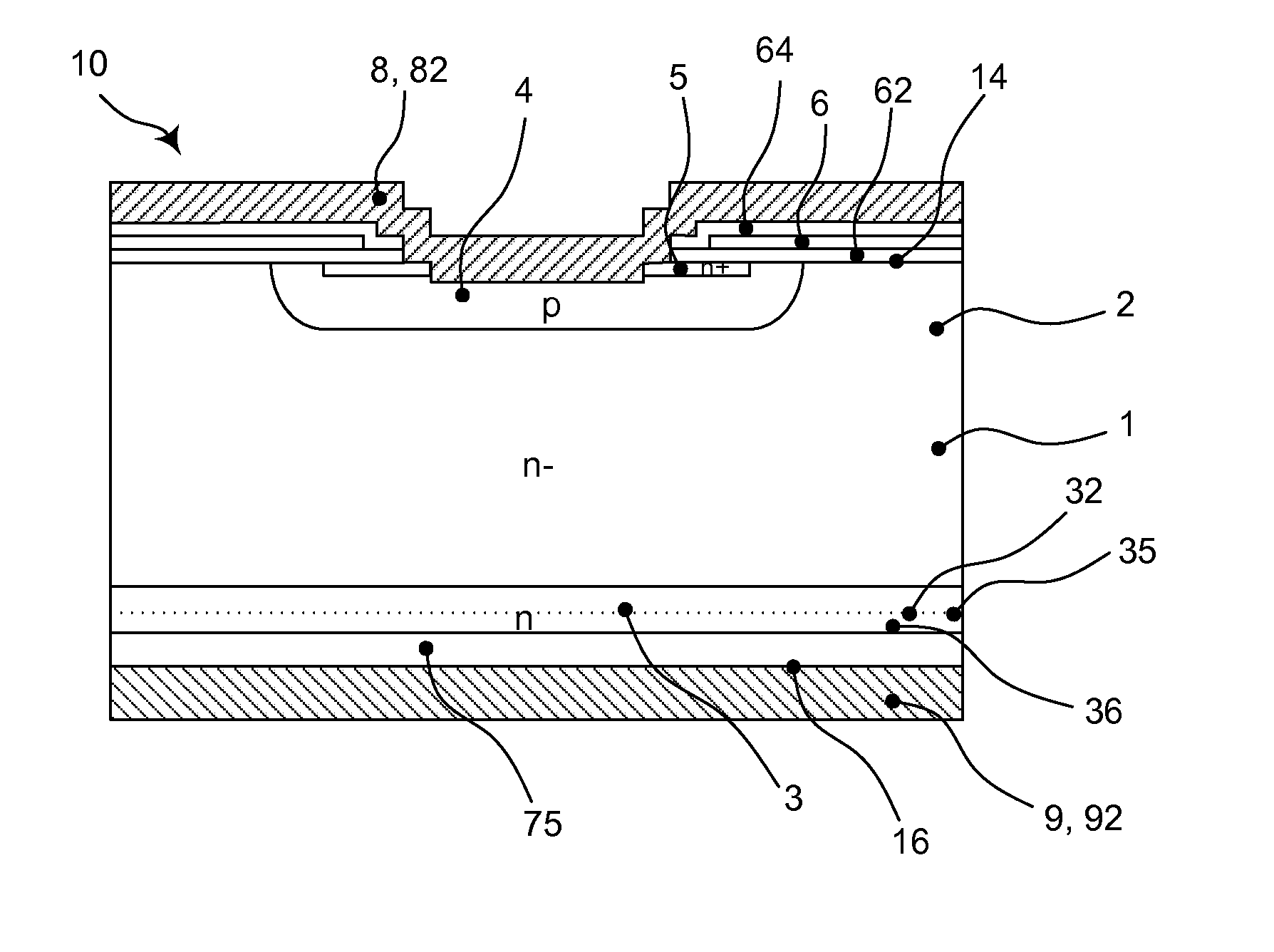
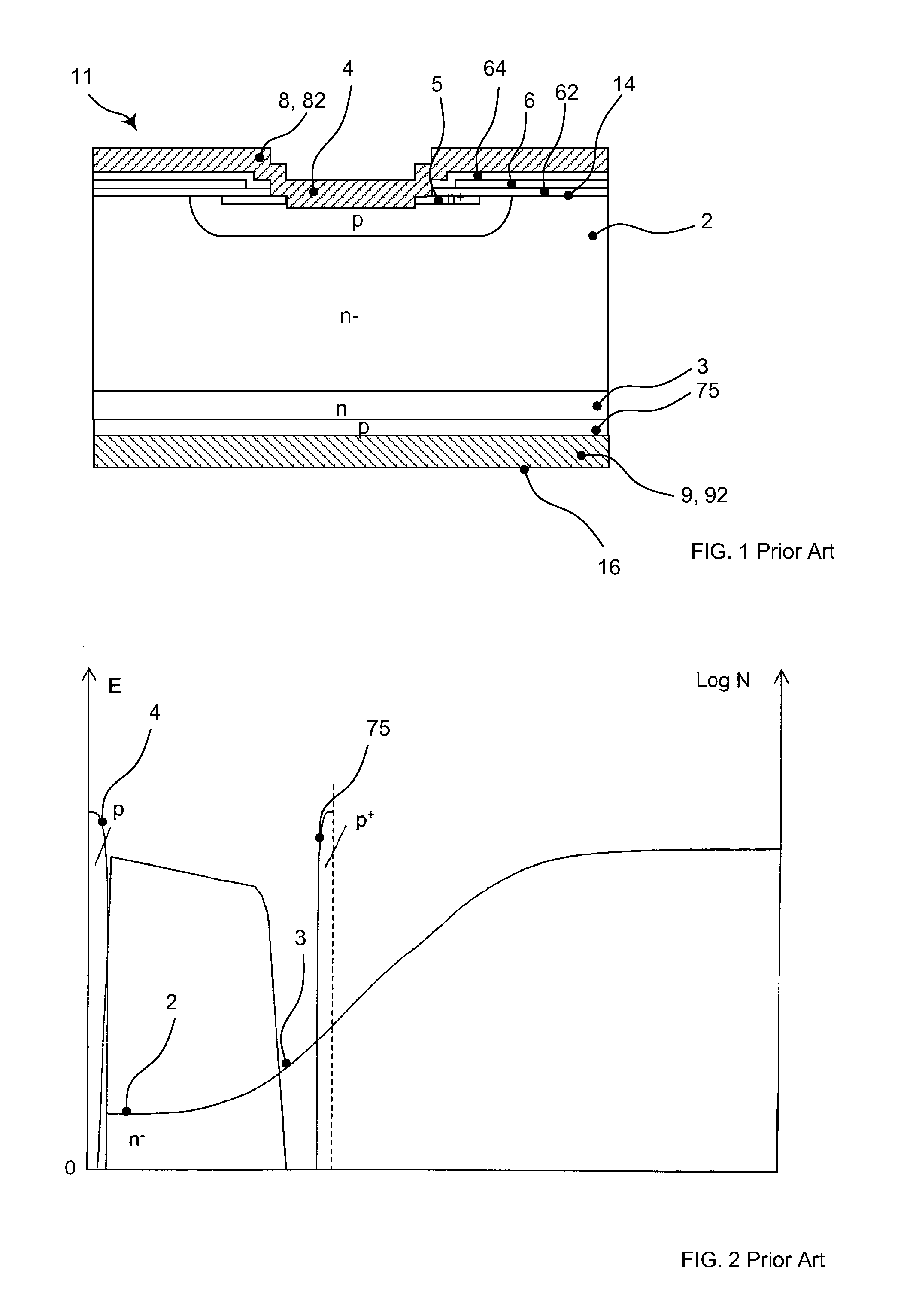
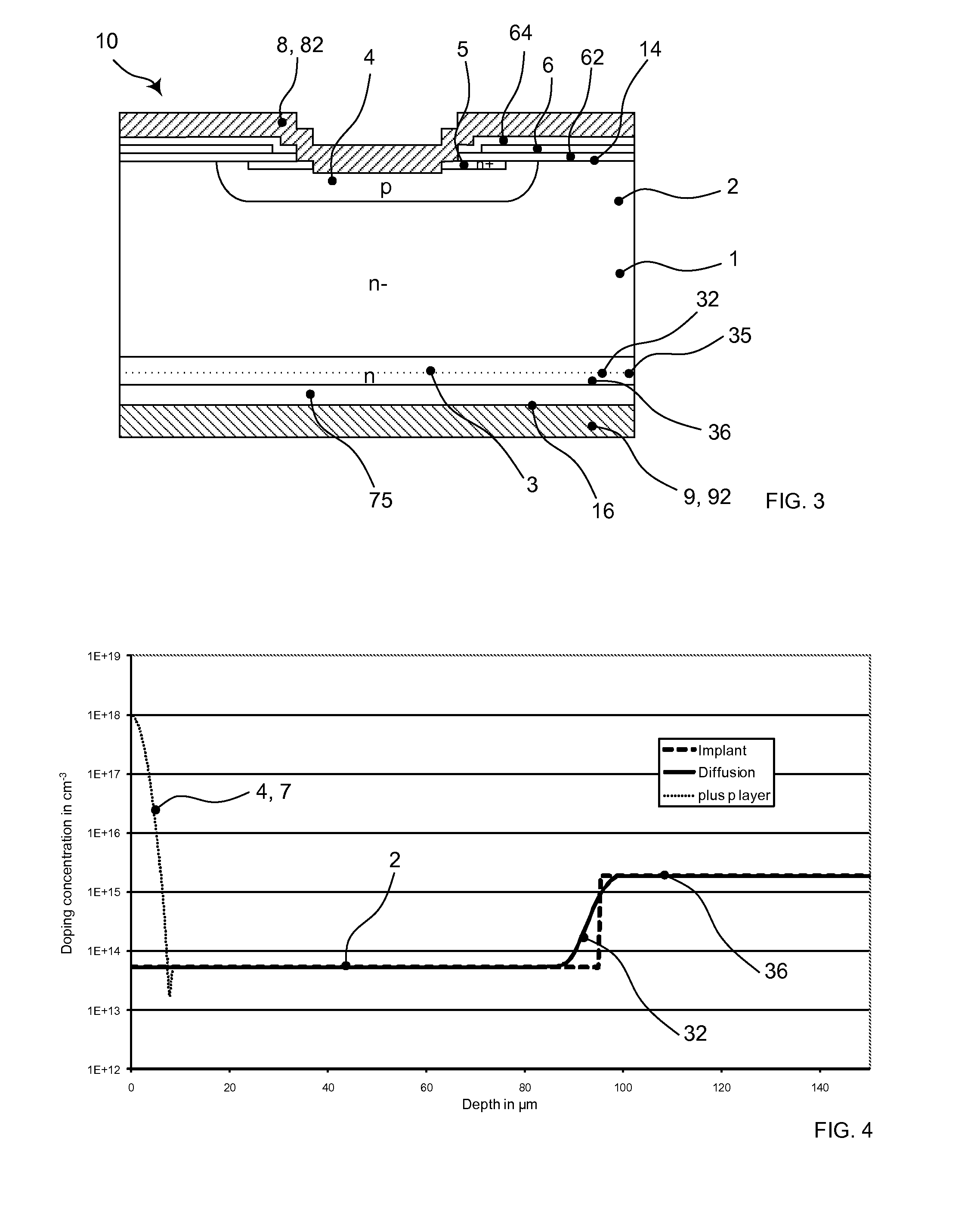
[0019]In accordance with an exemplary embodiment, a method is disclosed for manufacturing a bipolar punch-through semiconductor device, which is applicable for low-voltage devices and by which method a better controllability of the manufacturing method itself and consequently of the electrical properties of the device are achievable.

[0020]In accordance with an exemplary embodiment, a method for manufacturing a bipolar punch-through semiconductor device with a semiconductor wafer is disclosed, which can include, depending on the semiconductor type, at least a two-layer structure with layers of a first and a second conductivity type, which second conductivity type is different from the first conductivity type, wherein one of the layers is a drift layer of the first conductivity type.

[0021]In accordance with an exemplary embodiment, a method is disclosed, which can include the following manufacturing steps:

[0022](a) providing a wafer with a wafer thickness, which has a first side and a...


PUM


Abstract

A method for manufacturing a bipolar punch-through semiconductor device is disclosed, which includes providing a wafer having a first and a second side, wherein on the first side a high-doped layer of the first conductivity type having constant high doping concentration is arranged; epitaxially growing a low-doped layer of the first conductivity type on the first side; performing a diffusion step by which a diffused inter-space region is created at the inter-space of the layers; creating at least one layer of the second conductivity type on the first side; and reducing the wafer thickness within the high-doped layer on the second side so that a buffer layer is created, which can include the inter-space region and the remaining part of the high-doped layer, wherein the doping profile of the buffer layer decreases steadily from the doping concentration of the high-doped region to the doping concentration of the drift layer.

Description

RELATED APPLICATION(S)[0001]This application claims priority as a continuation application under 35 U.S.C. §120 to PCT / EP2012 / 056456, which was filed as an International Application on Apr. 10, 2012, designating the U.S., and which claims priority to European Application No. 11161304.8 filed in Europe on Apr. 6, 2011. The entire contents of these applications are hereby incorporated herein by reference in their entireties.FIELD[0002]The disclosure relates to the field of power electronics and for example to a method for manufacturing a bipolar punch-through semiconductor device and to a bipolar punch-through semiconductor device.BACKGROUND INFORMATION[0003]In EP 1 017 093 A1, a method for manufacturing an IGBT having an emitter side 14 and a collector side 16 is described. On the collector side 16 of a wafer an n doped layer is created by diffusion. On the emitter side 14, a p-base layer 4, n source regions 5 and a gate electrode 6 are then created. Afterwards an emitter electrode 8...

Claims


Application Information

Patent Timeline
Patent Type & Authority Applications(United States)
IPC IPC(8): H01L29/66H01L29/739
CPCH01L29/66325H01L29/7393H01L29/6609H01L29/0834H01L29/36H01L29/66136H01L29/66333H01L29/66348H01L29/7395H01L29/7397H01L29/861H01L21/18H01L29/739
Inventor RAHIMO, MUNAFKOPTA, ARNOSTCLAUSEN, THOMASANDENNA, MAXI
Owner HITACHI ENERGY SWITZERLAND AG
Why Eureka
Try Eureka