Electrode composite and photoelectric element equipped therewith

a technology of photoelectric elements and composites, which is applied in the direction of electrolytic capacitors, thermoelectric devices, capacitors, etc., can solve the problems that the technique described in the patent literature 1 should not improve the conversion efficiency, interfere with electron transfer, etc., and achieve high electron transport properties, large area, and high electron transport properties

Active Publication Date: 2014-02-20
PANASONIC CORP +1
View PDF3 Cites 17 Cited by
  • Summary
  • Abstract
  • Description
  • Claims
  • Application Information

AI Technical Summary

Benefits of technology

[0012]The first invention and the second invention can provide an electrode composite that can constitute a photoelectric element having a reaction interface with a large area and having high electron transport properties between the reaction interface and an electrode.
[0013]The third invention can provide a photoelectric element that includes the electrode composite and has a reaction interface with a large area and high electron transport properties between the reaction interface and an electrode.

Problems solved by technology

However, by the technique described in Patent literature 1, it is supposed that electrons excited by incident light are trapped by the conductive material having a high electric conductivity during the transfer of electrons in the semiconductor for a photoelectric conversion material including the semiconductor such as titanium oxide adsorbing a dye and the conductive material such as tin oxide, and this interferes with the electron transfer.
On this account, the technique described in Patent literature 1 should not improve conversion efficiency.

Method used


Image

  • Electrode composite and photoelectric element equipped therewith
  • Electrode composite and photoelectric element equipped therewith
  • Electrode composite and photoelectric element equipped therewith

Examples


example 1

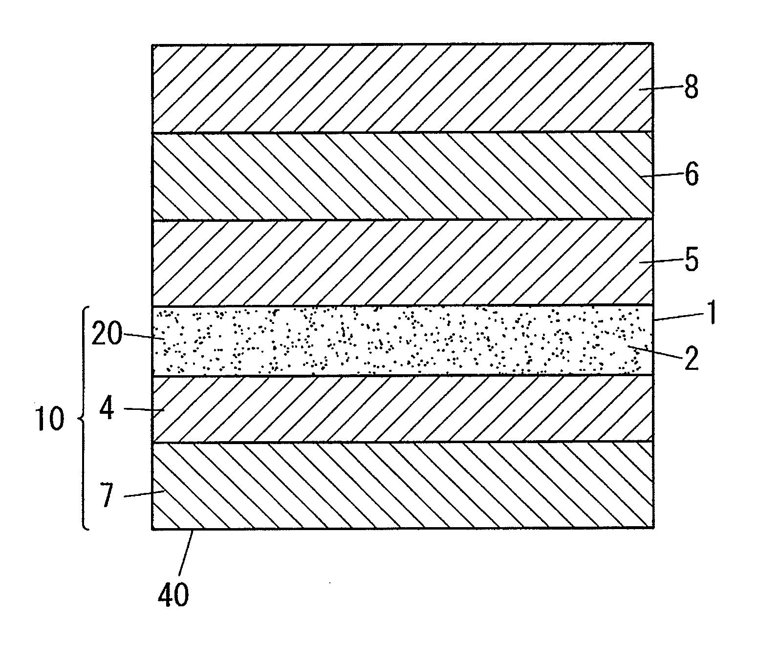
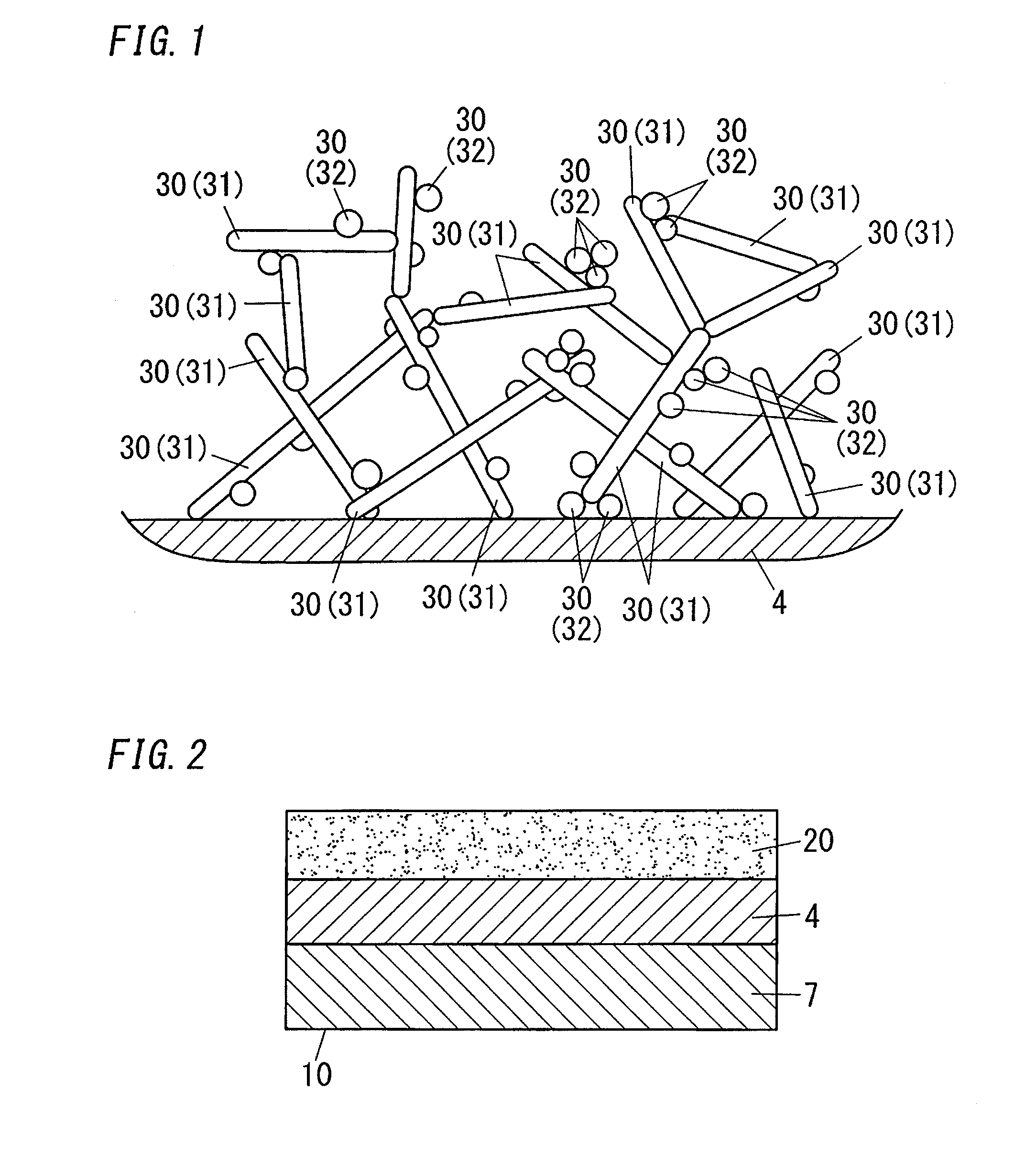
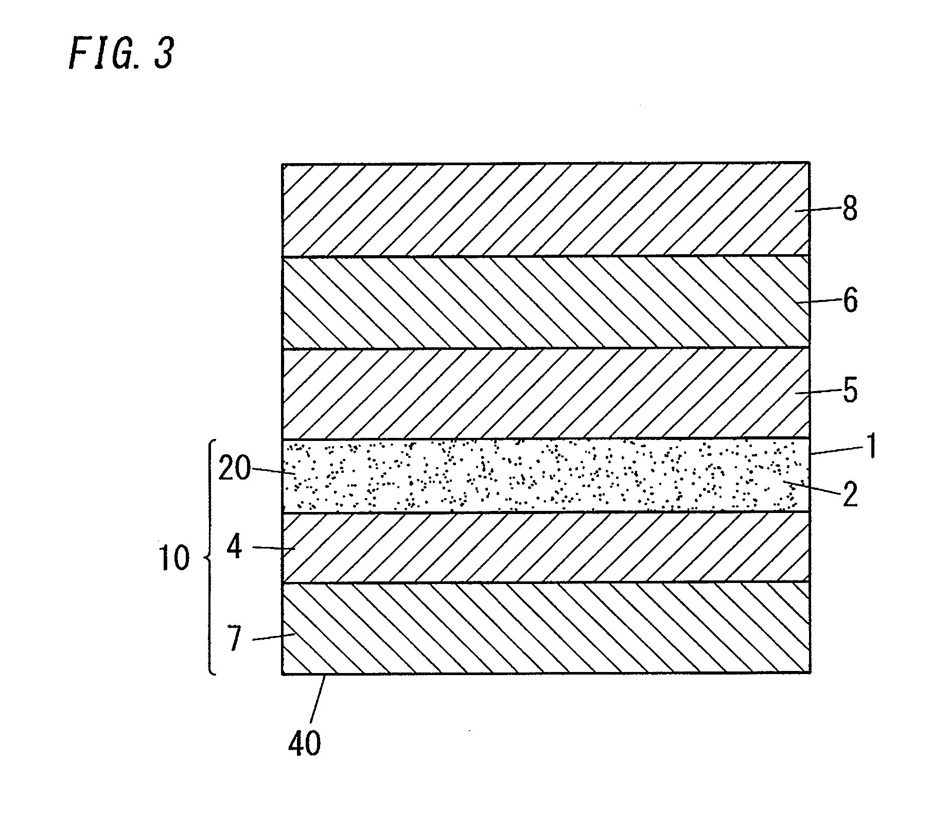
[0145]An electrically conductive glass substrate having a thickness of 0.7 mm and a sheet resistance of 100 Ω / sq. was prepared. The electrically conductive glass substrate includes a glass substrate and a coating film of fluorine-doped SnO2 stacked on a face of the glass substrate. The glass substrate and the coating film of the electrically conductive glass substrate are a first substrate and a first electrode, respectively.

[0146]Mixing 10 ml of dispersion liquid containing 30 wt % acicular antimony trioxide (ATO) particles in methyl ethyl ketone, 3 g of indium-tin oxide (ITO) paste, and a binder (methyl methacrylate polymer; PMMA) prepared a mixed liquid. The mixed liquid contains acicular ATO particles, spherical ITO particles, and PMMA in a mass ratio of 30:30:40. The acicular ATO particles have an average major axis length of 0.14 μm and an average minor axis length of 0.015 nm. The spherical ITO particles have an average particle size of 20 nm.

[0147]The mixed liquid was applie...

examples 2 and 3

[0148]An electrode composite was obtained in the same condition as in Example 1 except that the ratio of the acicular ATO particles, the spherical ITO particles, and PMMA in the mixed liquid for forming the conductive particle layer was changed as shown in Table 1.

example 4

[0149]An electrode composite was obtained in the same condition as in Example 1 except that the acicular ATO particles were replaced with acicular indium-tin oxide (ITO) particles having an average major axis length of 700 nm and an average minor axis length of 68 nm.


PUM

PropertyMeasurementUnit
pore sizeaaaaaaaaaa
lengthaaaaaaaaaa
particle sizeaaaaaaaaaa

Abstract

The present invention provides an electrode composite that has a reaction interface with a large area and can constitute a photoelectric element having high electron transport properties between the reaction interface and the electrode. The electrode composite of the present invention includes a first electrode and a conductive particle layer stacked on the first electrode. The conductive particle layer includes conductive particles containing acicular particles. The conductive particle layer has a three-dimensional porous network structure that is formed by the interconnection of the conductive particles. The three-dimensional network structure is joined to the first electrode. The conductive particle layer contains pores having a pore size of 50 nm or more in a total volume of 50% or more based on the volume of all pores in the conductive particle layer.

Description

TECHNICAL FIELD[0001]The present invention relates to an electrode composite and a photoelectric element equipped with the electrode composite and designed to convert light into electricity or electricity into light.BACKGROUND ART[0002]In recent years, photoelectric elements designed to convert light into electricity or electricity into light have been used as, for example, power generation devices (photoelectric conversion elements) by photoelectric conversion, such as a photovoltaic cell and a solar cell, light-emitting devices such as an organic EL device, optical display devices such as an electrochromic display device and electronic paper, and sensor devices designed to sense, for example, temperature and light.[0003]The photoelectric element includes an electron transport layer, which is required to have high electron transport properties. With respect to the electron transport layer, an area of a reaction interface as the interface on which charge separation or charge couplin...

Claims


Application Information

Patent Timeline
Patent Type & Authority Applications(United States)
IPC IPC(8): H01L51/52H01B1/00H01L51/44
CPCH01L51/5209H01B1/00H01L51/441H01L31/022425H01G9/2009H01G9/2022H01G9/2031H01G9/2059Y02E10/542H01B1/20Y02E10/549H10K85/141H10K85/151H10K85/631H10K30/82H10K2102/102H10K50/813H10K30/81
Inventor SUZUKA, MICHIOSEKIGUCHI, TAKASHINISHIDE, HIROYUKIOYAIZU, KENICHIKATO, FUMIAKI
Owner PANASONIC CORP
Why Eureka
Try Eureka