Film forming method
- Summary
- Abstract
- Description
- Claims
- Application Information
AI Technical Summary
Benefits of technology
Problems solved by technology
Method used
Image

Examples
Embodiment Construction
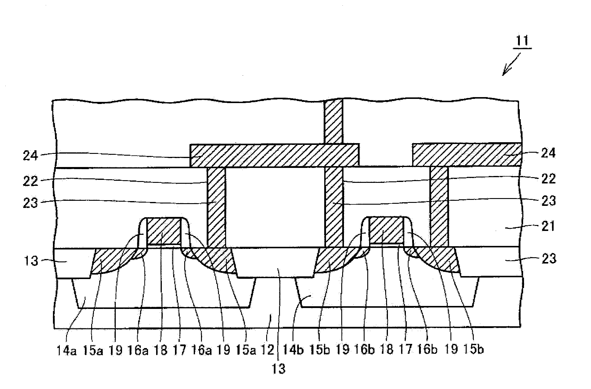
[0029]Hereinafter, exemplary embodiments of the present disclosure will be described with reference to accompanying drawings. First, a configuration of a semiconductor device having films formed by a film forming method according to an exemplary embodiment of the present disclosure will be described. FIG. 1 is a schematic cross-sectional view illustrating a portion of a MOS type semiconductor device. In the MOS type semiconductor device illustrated in FIG. 1, conductive layers are indicated by hatching.
[0030]Referring to FIG. 1, the MOS type semiconductor device 11 is formed with an element isolation region 13, a p-type well 14a, an n-type well 14b, a high density n-type impurity diffusion region 15a, a high density p-type impurity diffusion region 15b, an n-type impurity diffusion region 16a, a p-type impurity diffusion region 16b, and a gate oxide film 17, on a silicon substrate 12. The high density n-type impurity diffusion region 15a and the high density p-type impurity diffusio...
PUM
| Property | Measurement | Unit |
|---|---|---|
| Energy | aaaaa | aaaaa |
| Electron concentration | aaaaa | aaaaa |
| Adsorption entropy | aaaaa | aaaaa |
Abstract
Description
Claims
Application Information
 - Generate Ideas
- Intellectual Property
- Life Sciences
- Materials
- Tech Scout
- Unparalleled Data Quality
- Higher Quality Content
- 60% Fewer Hallucinations
Browse by: Latest US Patents, China's latest patents, Technical Efficacy Thesaurus, Application Domain, Technology Topic, Popular Technical Reports.
© 2025 PatSnap. All rights reserved.Legal|Privacy policy|Modern Slavery Act Transparency Statement|Sitemap|About US| Contact US: help@patsnap.com