Compound semiconductor epitaxial structure and method for fabricating the same

a semiconductor and epitaxial structure technology, applied in the field of semiconductor devices, can solve problems such as delamination problems

Active Publication Date: 2014-03-13
UNITED MICROELECTRONICS CORP
View PDF4 Cites 56 Cited by
  • Summary
  • Abstract
  • Description
  • Claims
  • Application Information

AI Technical Summary

Benefits of technology

[0006]In accordance with an aspect, the present invention provides a method for fabricating a compound semiconductor epitaxial structure. The method includes the following steps. Firstly, a first compound epitaxial layer is formed on a substrate. Then, a continuous epitaxial deposition proc

Problems solved by technology

Moreover, since the lattice constant of silicon is different from that of germanium, the interfacial lattice mismatch between the silicon germanium epitaxial structure and the silicon substrate, a

Method used


Image

  • Compound semiconductor epitaxial structure and method for fabricating the same
  • Compound semiconductor epitaxial structure and method for fabricating the same
  • Compound semiconductor epitaxial structure and method for fabricating the same

Examples


Embodiment Construction

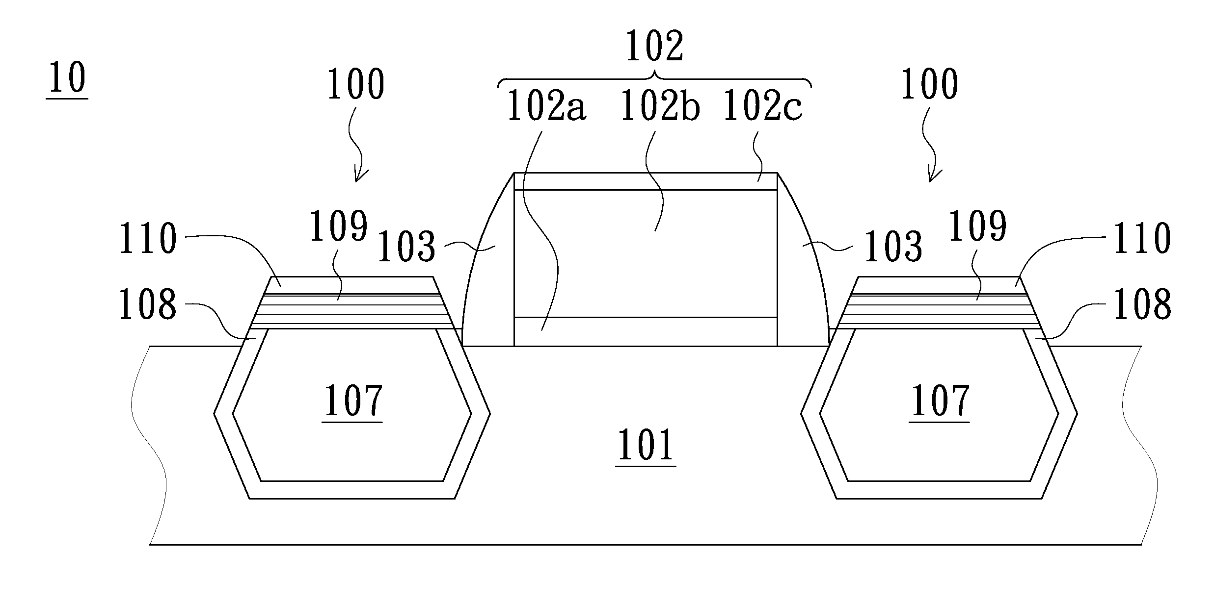
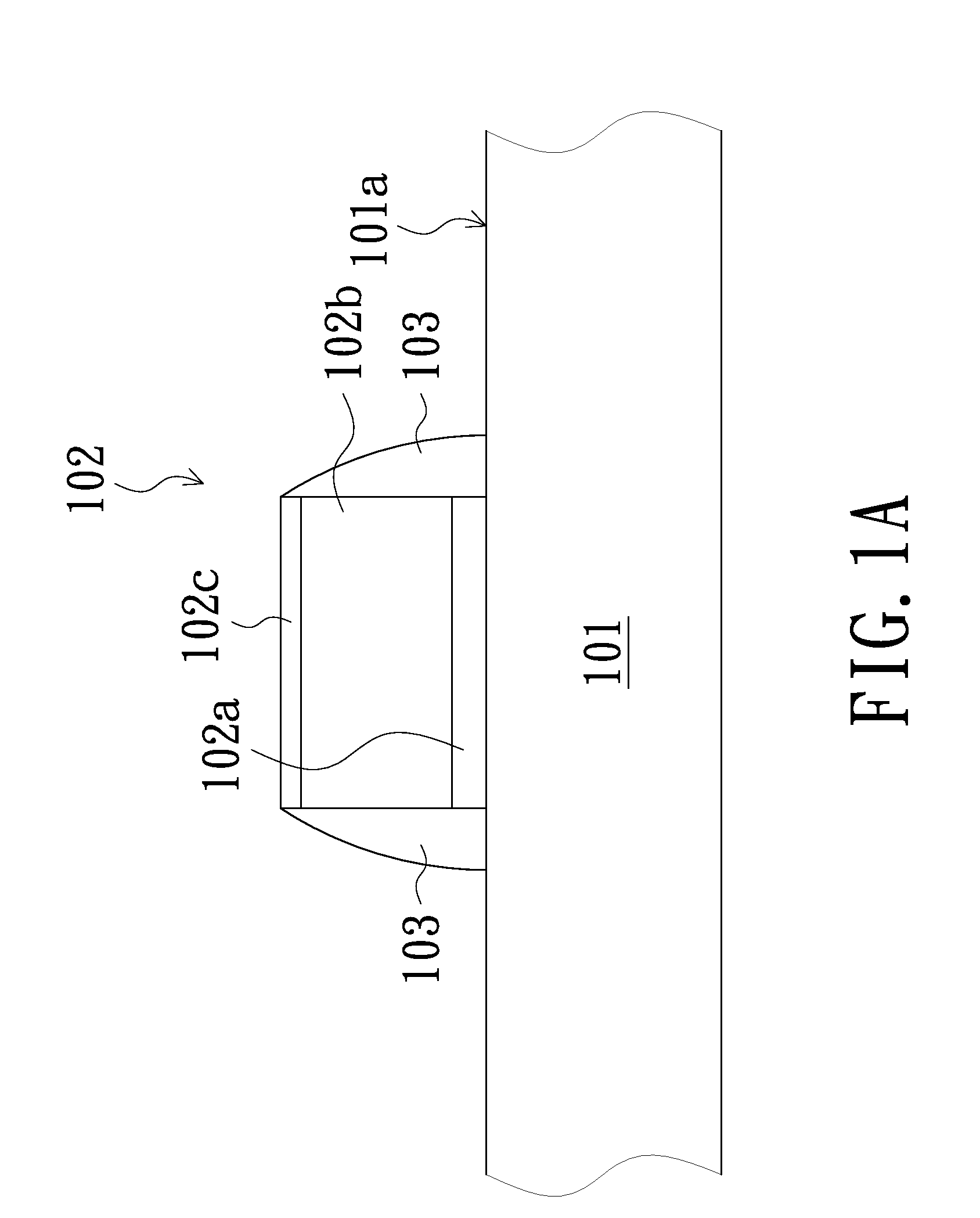
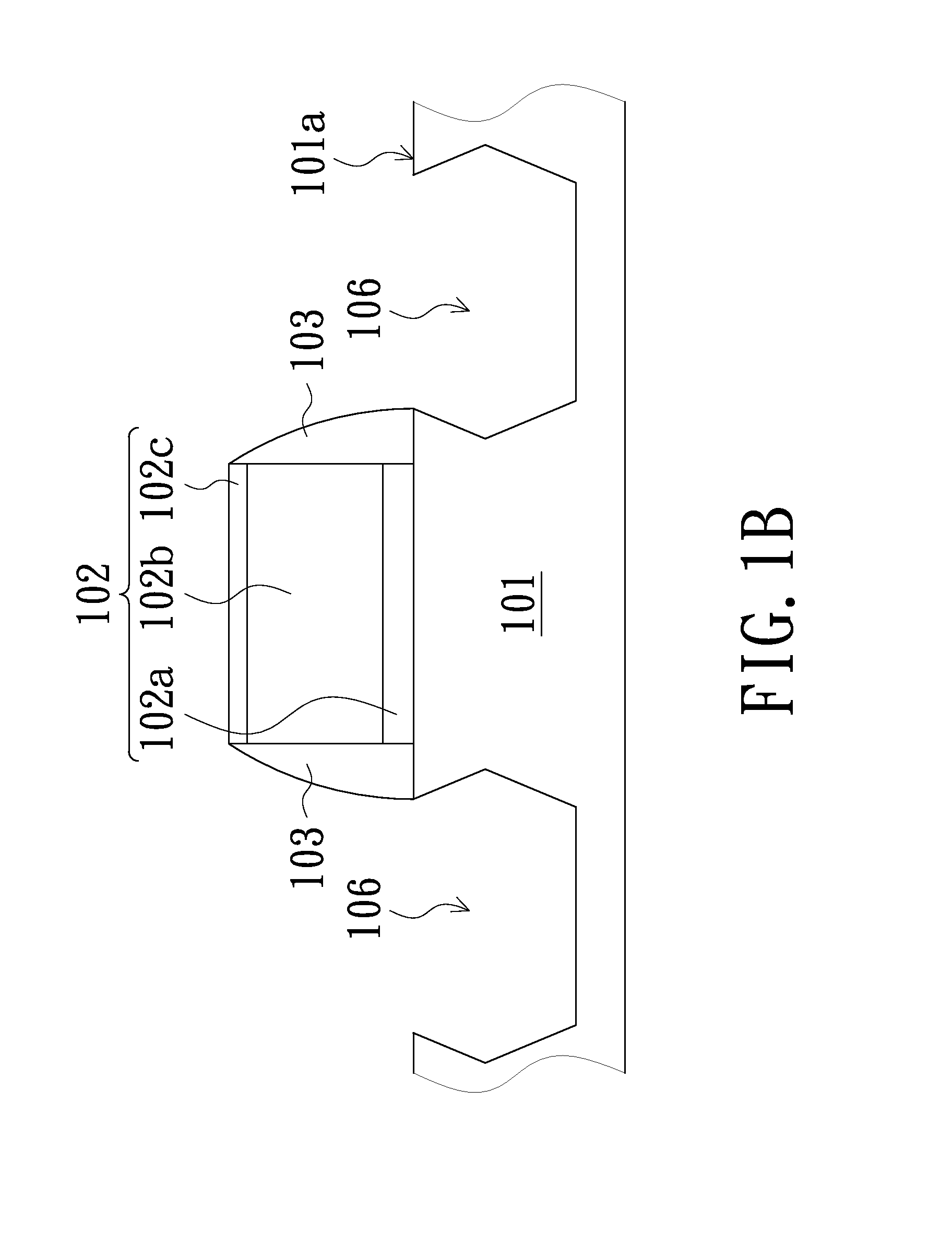
[0032]The present invention will now be described more specifically with reference to the following embodiments. It is to be noted that the following descriptions of preferred embodiments of this invention are presented herein for purpose of illustration and description only. It is not intended to be exhaustive or to be limited to the precise form disclosed.

[0033]As previously described herein, the interfacial lattice mismatch may result in stress relaxation of the compound epitaxial structure and thereby reduce the device performance. For solving the above drawbacks, the present invention provides a compound semiconductor epitaxial structure and a method for fabricating the compound semiconductor epitaxial structure. The above and other objects, features and advantages of the present invention will become more readily apparent to those ordinarily skilled in the art after reviewing the following detailed description and accompanying drawings. An embodiment of a method for fabricatin...


PUM


Abstract

A method for fabricating a compound semiconductor epitaxial structure includes the following steps. Firstly, a first compound epitaxial layer is formed on a substrate. Then, a continuous epitaxial deposition process is performed to form a second compound epitaxial layer on the first compound epitaxial layer, so that the second compound epitaxial layer has a linearly-decreased concentration gradient of metal. Afterwards, a semiconductor material layer is formed on the second compound epitaxial layer.

Description

FIELD OF THE INVENTION[0001]The present invention relates to a semiconductor device and a method for fabricating the semiconductor device, and more particularly to a compound semiconductor epitaxial structure and a method for fabricating the compound semiconductor epitaxial structure.BACKGROUND OF THE INVENTION[0002]With the technological advances of the communication equipment and other electronic equipment, the operating speed of the semiconductor device becomes faster and faster. For increasing the mobility of electrons and holes in the semiconductor device, compound semiconductor epitaxial structures are widely used in a variety of semiconductor applications. For example, the compound semiconductor epitaxial structure may be used in the fabrication of a metal-oxide-semiconductor field-effect transistor (MOSFET).[0003]Because the lattice constant of the silicon germanium epitaxial material is larger than that of the monocrystalline silicon substrate, a compressive stress may be a...

Claims


Application Information

Patent Timeline
IPC IPC(8): C30B25/14H01L29/36
CPCC30B25/165C30B29/52H01L21/02381H01L21/0245H01L21/02505H01L21/0251H01L21/02532H01L21/02579H01L21/0262H01L21/02639H01L29/66628H01L29/66636H01L29/7848
Inventor YU, TIEN-WEICHIEN, CHIN-CHENGLAI, I-MINGCHEN, SHIN-CHILI, CHIH-YUEHCHUANG, FONG-LUNGLIAO, CHIN-ILIN, KUAN-YU
Owner UNITED MICROELECTRONICS CORP
Why Eureka
Try Eureka