Circuit board with twinned cu circuit layer and method for manufacturing the same

a technology of circuit layer and circuit layer, which is applied in the direction of electrical apparatus, semiconductor devices, semiconductor/solid-state device details, etc., can solve the problems of under-performing ability to resist electromigration, increasing manufacturing cost, and less noticeable value of actual application in reality, so as to reduce production cost, reduce production cost, and accelerate the effect of deposition rate and speed ra

Active Publication Date: 2014-04-17
NAT CHIAO TUNG UNIV
View PDF2 Cites 15 Cited by
  • Summary
  • Abstract
  • Description
  • Claims
  • Application Information

AI Technical Summary

Benefits of technology

[0022]The time required for the method for manufacturing the current invention is shorter than the physical vapor deposition method required for the known technology, and the deposition rate and speed rate are faster. The expensive vapor phase deposition equipment is not required, therefore, this can greatly reduce the production cost. In addition, the present invention can also produce in a simple manner nano twinned copper having high density and [111] preferred orientation, which has, in addition to excellent mechanical properties (higher elastic modulus), higher electromigration resistance capability as increased by twinned crystals arrangement, which all can contribute to increasing product liability and especially applicability to manufacture of integrated circuit.

Problems solved by technology

However, the copper lines prepared as above described method usually have the issue of under-performing capability to resist electromigration.
However, this method has the potential problem of suffering from contamination, or increasing cost of manufacture, the value of actual application in reality is instead less noticeable.
However, the nanoscale twinned copper formed by the physical vapor deposition has short crystal lattice having scattered orientation led to by undefinable copper lattice direction.
As such, the twins' density is relatively low, and therefore cannot work to lead to significant improvement on electromigration resistance capability and ultimately failing to create actual utility value.
In addition, when physical vapor deposition is used to form twinned copper structure, the time for deposition is a lengthy undertaking, and cannot work to plate into vias or trenches having high aspect ratio, this method therefore cannot be directly applied in copper interconnect, copper wires, or through-silicon via (TSV).

Method used


Image

  • Circuit board with twinned cu circuit layer and method for manufacturing the same
  • Circuit board with twinned cu circuit layer and method for manufacturing the same
  • Circuit board with twinned cu circuit layer and method for manufacturing the same

Examples


embodiment 1

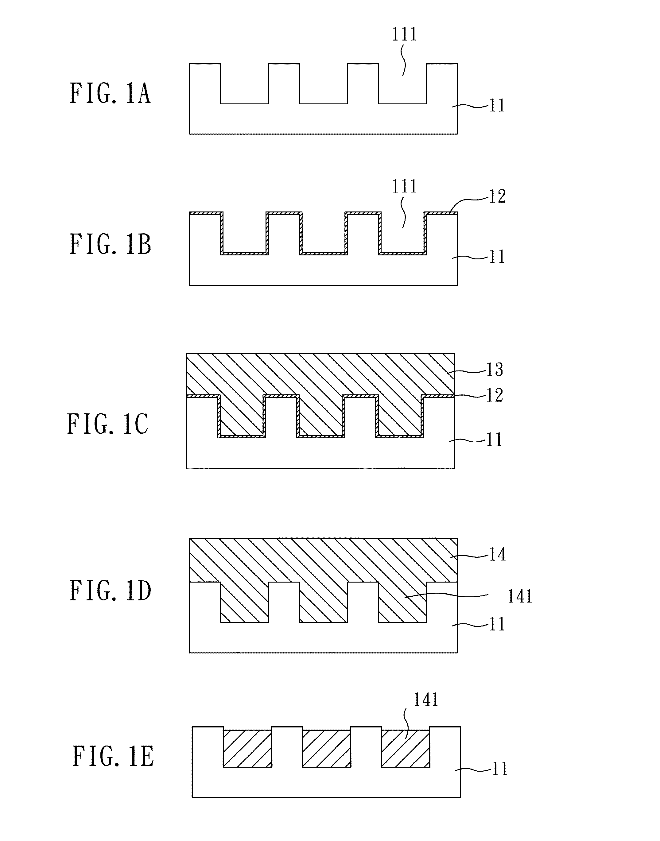
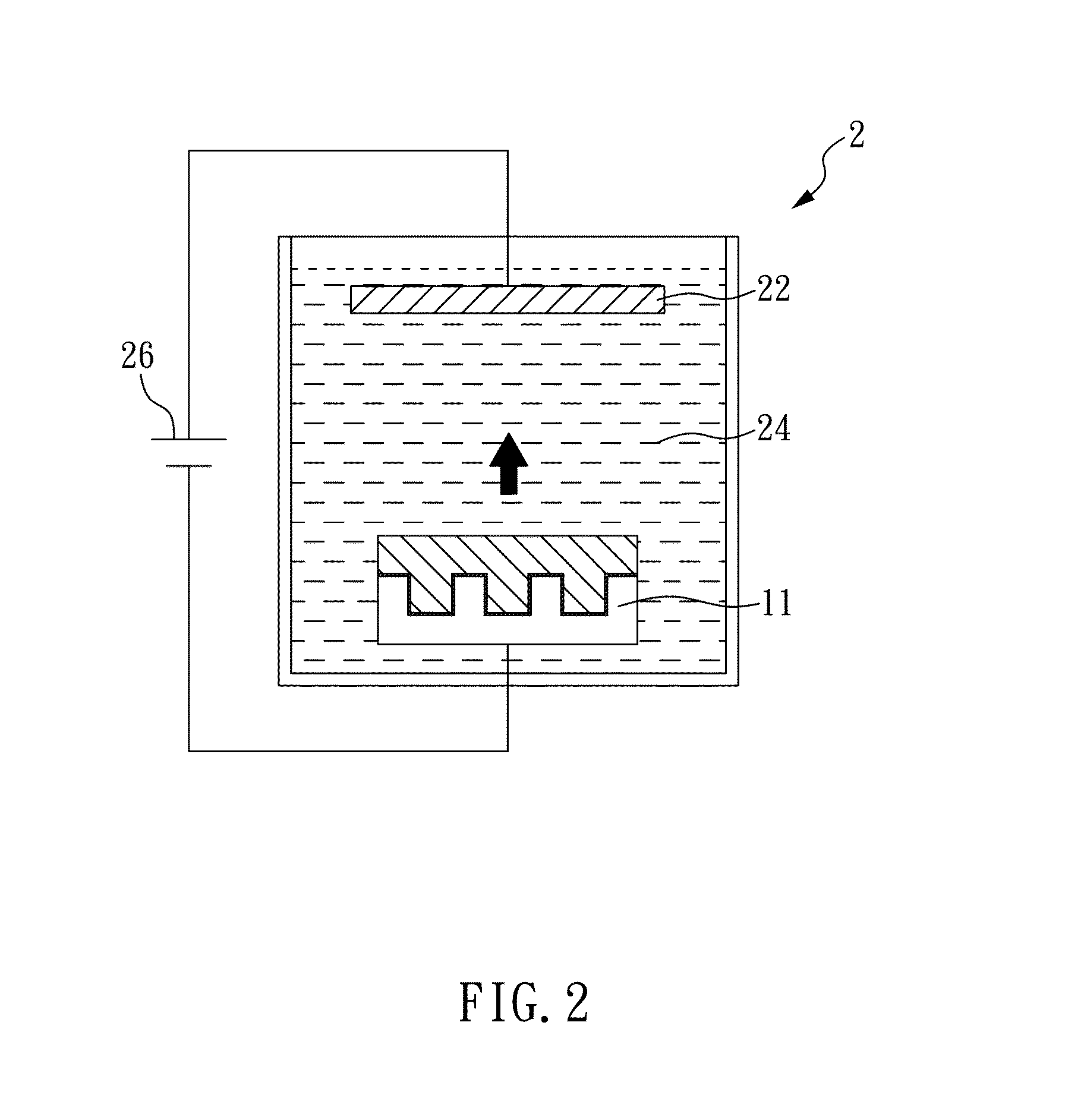
[0032]FIGS. 1A to 1D are cross-sectional views of a process for manufacturing the copper circuit layer of the present embodiment. FIG. 2 is a schematic view of an electroplating device for forming copper circuit layer of the present embodiment.

[0033]As shown in FIG. 1A, the first step of the method is to provide a silicon substrate 11, on which a surface is disposed with multiple trenches 111, and the height and depth of the each trenches is 0.8 μm and 0.8 μm respectively. The next step is to use the electroplating device shown in FIG. 2 to carry out electroplating on the silicon substrate 11. As shown in FIG. 2, the silicon substrate is placed in an electroplating device 2 as a cathode; wherein, the electroplating device 2 comprises an anode 22, which is immersed in an electroplating solution 24 and connected to a direct current electrical power 26 (Keithley 2400 is used in this case). The materials used for anode 22 can be metal copper, phosphor bronze or insert anode (e.g. titani...

embodiment 2

[0041]FIGS. 4A to 4E are cross-sectional views of the process for preparing circuit board of the present embodiment.

[0042]FIG. 4A begins with first providing a substrate 31, for which at least a surface is disposed with a first circuit layer, the first circuit layer is used as an electric attachment pad 32. This pad may connect to the active devices in the substrate. In the current embodiment, the substrate 31 is a circuit board having multiple layers of circuit; which will be shown here in drawings only, without description of detailed structure. In addition, the electric attachment pad 32 of the first circuit layer is manufactured by the same method for making circuit layer for embodiment 1, and the pad has nano twinned copper structure.

[0043]And then as shown in FIG. 4B, the next step is to form a first dielectric layer 33 on at least one surface of the substrate 31. Then, by way of the manufacturing process commonly used in the present invention technical field, such as photolit...

embodiment 3

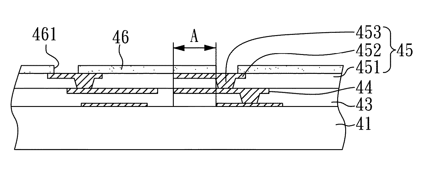
[0048]FIG. 5A to 5B are cross-sectional views of a process for preparing the circuit board of embodiment 3 according to the present invention.

[0049]As shown in FIG. 5A, the circuit board of the present invention comprises: a substrate 41, the surface of which has a first circuit layer, and the first circuit layer comprises an electrical attachment pad 42; a first dielectric layer 43, which is disposed on a surface of the substrate 41 and the first circuit layer; and a second circuit layer 44, which is formed on a surface of the first dielectric layer 43, the second circuit layer 44 comprises multiple first conductive vias 441 and a first circuit 442, the first conductive via 441 communicates and is electrically connected to the electrical attachment pad 42. Here, the manufacturing method and conditions for the substrate, first dielectric layer 43 and second circuit layer 44 are the same as for Embodiment 2, further elaboration will be omitted here.

[0050]Furthermore, a built-up circu...


PUM


Abstract

A circuit board with twinned Cu circuit layer and a method for manufacturing the same are disclosed, wherein the method comprises the following steps: (A) providing a substrate with a first circuit layer formed thereon, wherein the first circuit layer comprises a conductive pad; (B) forming a first dielectric layer on the surface of the substrate; (C) forming plural openings in the first dielectric layer, wherein each opening penetrates through the first dielectric layer and communicates with the conductive pad to expose the conductive pad; (D) forming a Cu seeding layer in the openings; (E) forming a nano-twinned Cu layer in the openings with an electroplating process; and (F) annealing the substrate to transfer the material of the Cu seeding layer into nano-twinned Cu, wherein the nano-twinned Cu layer and the transferred Cu seeding layer are formed into a second circuit layer.

Description

CROSS-REFERENCE TO RELATED APPLICATIONS[0001]The present application claims the benefit of Taiwanese Patent Application No. 101138044, filed on Oct. 16, 2012, which is incorporated by reference in its entirety.BACKGROUND OF THE INVENTION[0002]The present invention relates to a circuit board with twinned copper circuit layer and method for manufacturing the same, particularly to a circuit board with twinned copper circuit layer for using on integrated circuit and method for manufacturing the same.[0003]With the rapid development of the electronics industry, demand for minimum volume, light weight; multifunction, and high-performing electronics has seen steady increased in quantity. On the current integrated circuit development, the semiconductor packaging technologies are applied now, in order to pack a number of active elements and passive elements onto the same device; therefore, an object having more circuits and electronic components are accommodated within a finite unit area can...

Claims


Application Information

Patent Timeline
Patent Type & Authority Applications(United States)
IPC IPC(8): H01L21/768H01L23/532
CPCH01L23/53238H01L21/76873H01L23/49822H01L23/49866H01L2924/0002H01L21/2885H01L21/76877H01L2924/00
Inventor CHEN, CHIHLIN, HAN-WEN
Owner NAT CHIAO TUNG UNIV
Why Eureka
Try Eureka