
Inorganic solution and solution process for electronic and electro-optic devices

a technology of electrooptic devices and inorganic solutions, applied in the direction of liquid/solution decomposition chemical coating, non-metal conductors, conductors, etc., can solve the problems of organic semiconductors still having problems with air stability stability, zinc or zinc chalcogenide cannot be dissolved into their hydrazine solution, and the cost reduction is not easy to achiev

Active Publication Date: 2014-05-01
RGT UNIV OF CALIFORNIA
View PDF3 Cites 4 Cited by
  • Summary
  • Abstract
  • Description
  • Claims
  • Application Information

AI Technical Summary

Benefits of technology

The patent text describes a solution for making a layer in an electronic or electro-optic device. The solution includes a solvent, an additive mixed with the solvent, and a solute dissolved in the solvent. The additive can be one of a variety of additives, and the solute can be a metal like copper, zinc, or tin, or a compound like selenium or tellurium. By depositing this solution on a substrate and heating it, a layer of Kesterite film can be formed. This solution can be used in the production of electronic or electro-optic devices, and the technical effect is that it provides a reliable and efficient way to produce a high-quality layer for use in these devices.

Problems solved by technology

However, the scaling up of production and the reduction of cost are still the main issues for photovoltaic technologies to compete with traditionally generated power (Contreras, M. A., Ramanathan, K., AbuShama, J., Hasoon, F., Young, D. L., Egaas, B., & Noufi, R., Prog.
Despite numerous advancements in this area, organic semiconductors still have problems with stability in air.
However, according to their approach, zinc or zinc chalcogenide cannot be dissolved into their hydrazine solutions.

Method used


Image

  • Inorganic solution and solution process for electronic and electro-optic devices
  • Inorganic solution and solution process for electronic and electro-optic devices
  • Inorganic solution and solution process for electronic and electro-optic devices

Examples


examples

[0026]The following examples help explain some concepts of the current invention. However, the general concepts of the current invention are not limited to the particular examples.

Procedures

Precursor Solution Preparation and Characterization

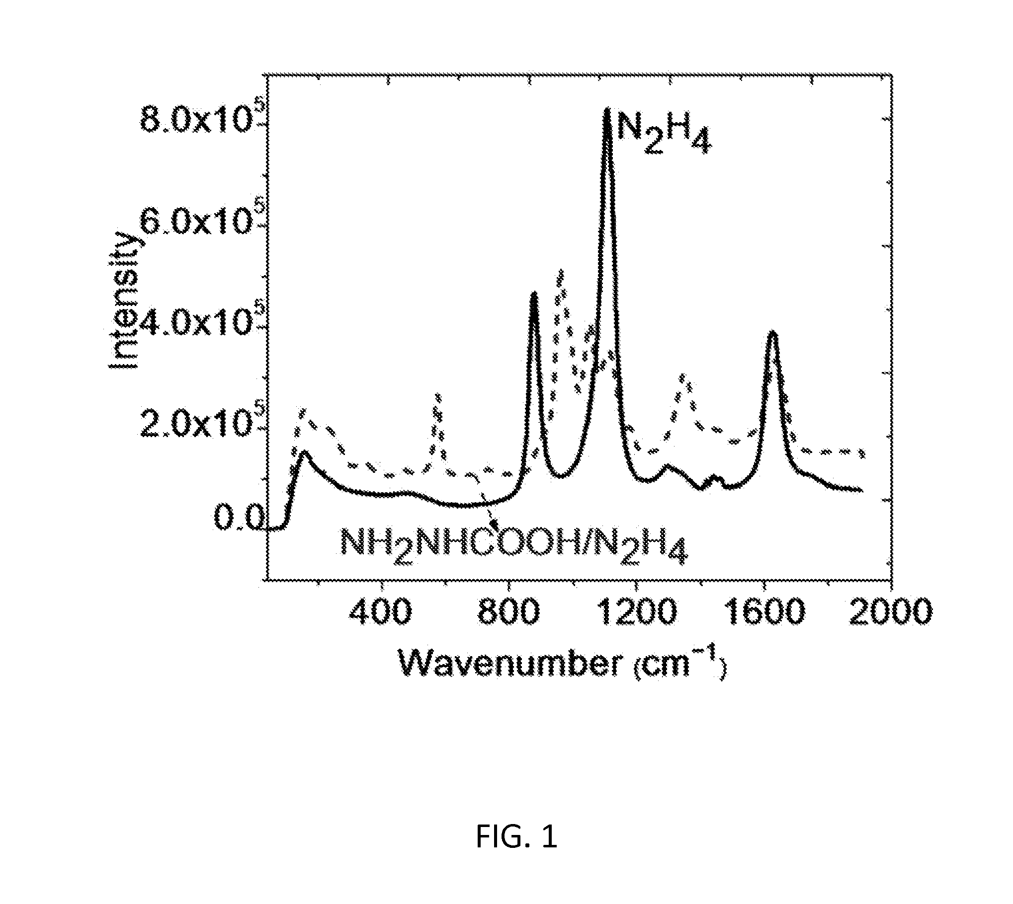
[0027]The mixture of hydrazine and hydrazine carboxylic acid is used as a solvent in this example. Hydrazine carboxylic acid is prepared by adding hydrazine into solid state carbon dioxide in a nitrogen filled dry box where oxygen and moisture levels are both below 0.1 ppm. The viscosity of the mixture liquid increases with the amount of carbon dioxide added. The desired precursor viscosity can be achieved by changing the ratio between hydrazine and hydrazine carboxylic acid. This can be an important advantage, especially for large-area device fabrication. The products of carbon dioxide and hydrazine were investigated by Raman spectroscopy.

[0028]Note: The reaction between carbon dioxide and hydrazine is highly exothermal, with a large amount of c...


PUM

PropertyMeasurementUnit
thicknessaaaaaaaaaa
pressureaaaaaaaaaa
pass energyaaaaaaaaaa

Abstract

A solution for forming at least a portion of an active layer of an electronic or electro-optic device includes a solvent, an additive mixed with the solvent to provide a solvent-additive blend, and a solute that includes at least one of a transition metal, an alkali metal, an alkaline earth metal, Al, Ga, In, Ge, Sn, or Sb dissolved in elemental form in the solvent-additive blend. The additive is selected from the group of additives consisting of NR1R2NHCOOH, NH2N—HCONHNH2, NH2COOH.NH3, NH2NHC(═NH)NH2.H2CO3, NH2NHCSNHNH2, NH2NHCSSH and all combinations thereof. R1 and R2 are each independently selected from hydrogen, aryl, methyl, ethyl and a linear, branched or cyclic alkyl of 3-6 carbon atoms. Methods of producing the solution, a method of producing a Kesterite film on a substructure and devices made with the solutions and methods are also provided.

Description

CROSS-REFERENCE OF RELATED APPLICATION[0001]This application claims priority to U.S. Provisional Application No. 61 / 498,295 filed Jun. 17, 2011, the entire contents of which are hereby incorporated by reference.BACKGROUND[0002]1. Field of Invention[0003]The field of the currently claimed embodiments of this invention relates to inorganic solutions and solution processes for producing electronic and / or electro-optic devices and devices made by the solutions and processes.[0004]2. Discussion of Related Art[0005]Due to the general concern over global warming, and increasing demand for energy, much research has focused on developing a feasible method for renewable energy generation. Among renewable energy sources, solar energy has attracted the most attention due to the direct conversion of energy to electricity from the sun. However, the scaling up of production and the reduction of cost are still the main issues for photovoltaic technologies to compete with traditionally generated pow...

Claims


Application Information

Patent Timeline
Patent Type & Authority Applications(United States)
IPC IPC(8): H01L31/032H01L31/18
CPCH01L31/0326H01L31/18C23C18/1204H01B1/02H01B1/22H01L21/02557H01L21/0256H01L21/02568H01L21/02628Y02E10/50
Inventor YANG, YANGYANG, WENBINGLI, SHENGHANHSU, WAN-CHING
Owner RGT UNIV OF CALIFORNIA
Learn More