Capacitively coupled plasma equipment with uniform plasma density

a plasma density and capacitive coupling technology, applied in the field of plasma processing, can solve the problems of complex and expensive attempts, non-uniformity of plasmas of higher frequency, and significant challenge of plasma non-uniformity, and achieve the effect of enhancing the vapor deposition of plasma

Inactive Publication Date: 2014-05-22
TOKYO ELECTRON LTD
View PDF4 Cites 25 Cited by
  • Summary
  • Abstract
  • Description
  • Claims
  • Application Information

AI Technical Summary

Benefits of technology

[0005]Plasma etching of semiconductor wafers, as well as plasma-enhanced chemical vapor deposition (PECVD), are commonly executed using a parallel plate capacitively coupled plasma tools. The semiconductor industry is moving toward making narrower or smaller nodes (critical features) on wafers, as well as using larger wafer sizes. For example, the industry is transitioning from working with 300 mm diameter wafers to 450 mm diameter wafers. With smaller node sizes and larger wafers, the macroscopic and microscopic uniformity of plasma and radicals becomes increasingly important to avoid defects in treated wafers.
[0008]Techniques disclosed herein include an upper electrode (hot electrode), of a capacitively coupled plasma system, with structural features configured to assist in generating a uniform plasma. Such structural features define a surface shape, on a surface that faces the plasma, which assists in disrupting standing waves and / or prevents standing waves from forming within the plasma space. For example, such structural features can include a set of concentric rings having an approximately rectangular cross section, and protruding from the surface of the upper electrode or defined within the surface of the electrode. The cross sectional size, shape, dimensions, as well as spacing of the rings, are all selected to result in a system that generates uniform density plasma. The upper electrode can include a dielectric member or sheet that covers the structural features and / or upper electrode that prevents or inhibits erosion of the structural features while still maintaining plasma uniformity. Main power for plasma generation can be supplied either to the upper or lower electrode, and bias power can be optionally supplied to the lower electrode. Such techniques can provide a uniform plasma even when using VHF power and or using electrodes with a relatively large surface area.
[0011]Another embodiment includes a method for generating a uniform plasma for processing a substrate using a plasma processing apparatus. The plasma processing apparatus including a vacuum-evacuable processing chamber, a lower electrode assembly disposed in the processing chamber and serving as a mounting table for a target substrate, an upper electrode disposed to face the lower electrode in the processing chamber, and a first radio frequency (RF) power supply connected to the upper electrode. The apparatus and electrodes can be sized sufficient for a particular application. For example, for wafer etching or CVD, electrodes can be sized to accommodate a 300 mm or 450 mm diameter wafer. For CVD on solar cells, electrodes can be sized substantially larger, such as having side dimensions of about 1-2 meters or more, and can be embodied as a single-piece electrode, instead of needing to be segmented into a group of electrodes. The first RF power supplies a first RF power to the upper electrode or to the lower electrode. A target substrate is loaded into the processing chamber and mounted on the lower electrode assembly. An initial gas is evacuated from the processing chamber. A processing gas is supplied into the processing chamber. A plasma is generated from the processing gas by applying the first RF power to the upper electrode (or to the lower electrode depending on a particular plasma system). The upper electrode has a surface area that faces the second electrode. The surface area is substantially planar and includes a set of concentric rings, nested rings or fins protruding from the surface area, the set of concentric rings is located at a predetermined spacing distribution, each concentric ring has a predetermined cross-sectional shape. A dielectric member or sheet can be positioned over the concentric rings and prevent or inhibit the plasma from eroding the concentric rings.

Problems solved by technology

In capacitively coupled plasma (CCP) systems, a significant challenge is plasma non-uniformity.
Such higher frequency plasmas, however, tend to be non-uniform at least in part due to a standing wave created in the plasma.
These attempts, however, are complicated and expensive.

Method used


Image

  • Capacitively coupled plasma equipment with uniform plasma density
  • Capacitively coupled plasma equipment with uniform plasma density
  • Capacitively coupled plasma equipment with uniform plasma density

Examples


Embodiment Construction

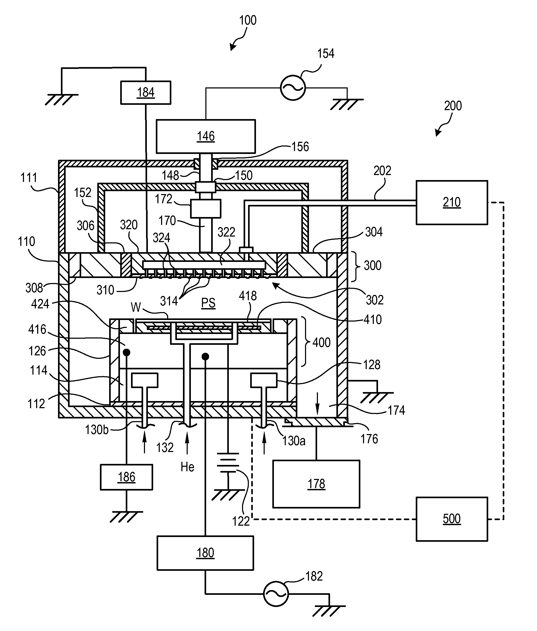
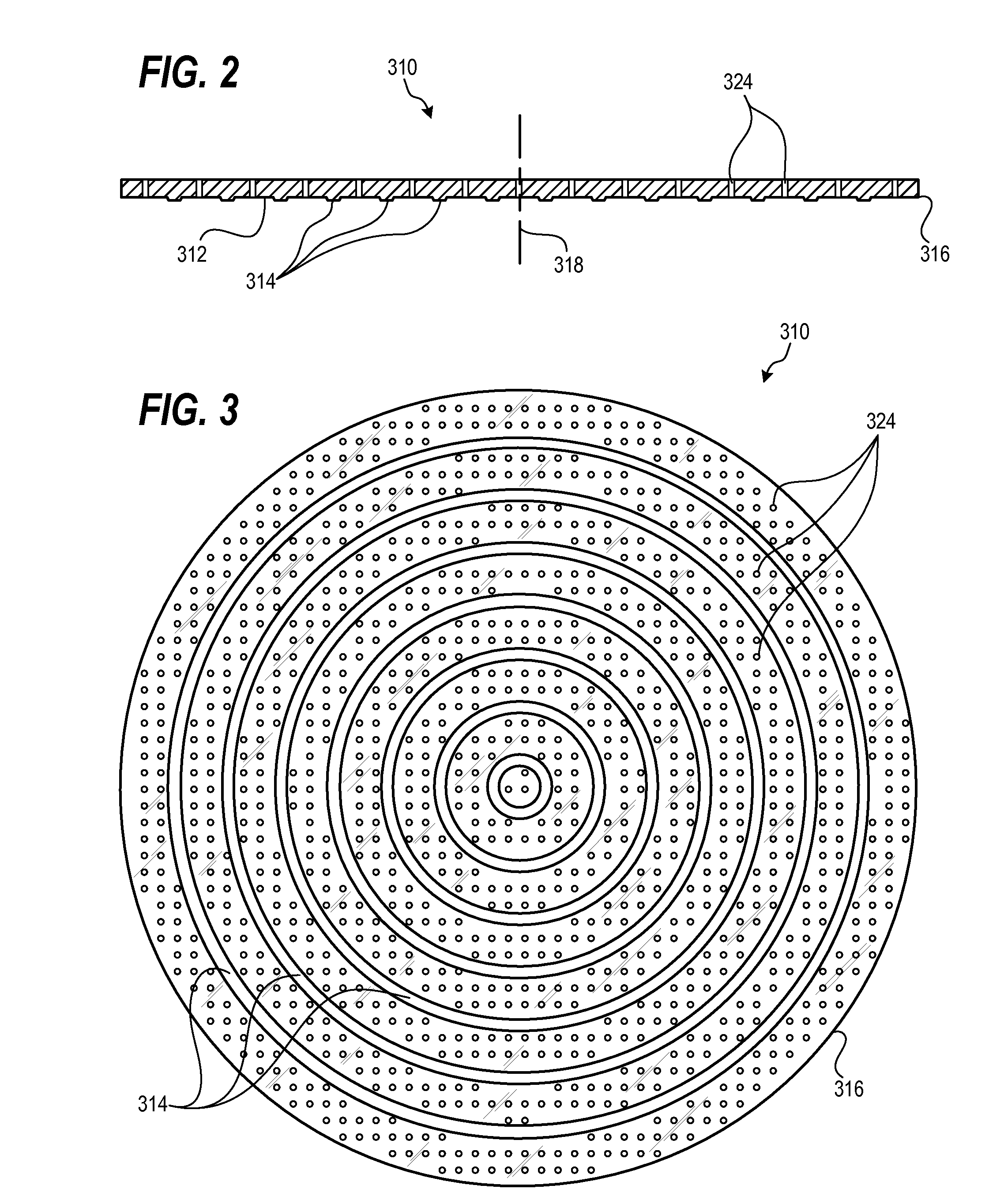
[0032]In the following description specific details are set forth, such as a particular geometry of a processing system and descriptions of various components and processes used therein. It should be understood, however, that the invention may be practiced in other embodiments that depart from these specific details, and that such details are for purposes of explanation and not limitation. Embodiments disclosed herein will be described with reference to the accompanying drawings. Similarly, for purposes of explanation, specific numbers, materials, and configurations are set forth in order to provide a thorough understanding. Nevertheless, embodiments may be practiced without such specific details. Components having substantially the same functional constructions are denoted by like reference characters, and thus any redundant descriptions may be omitted.

[0033]Various techniques will be described as multiple discrete operations to assist in understanding the various embodiments. The ...


PUM

PropertyMeasurementUnit
widthaaaaaaaaaa
widthaaaaaaaaaa
widthaaaaaaaaaa

Abstract

Techniques disclosed herein include apparatus and processes for generating plasma having a uniform electron density across an electrode used to generate the plasma. An upper electrode of a capacitively coupled plasma system can include structural features configured to assist in generating the uniform plasma. Such structural features define a surface shape, on a surface that faces the plasma. Such structural features can include a set of concentric rings having an approximately rectangular cross section, and protruding from the surface of the upper electrode. Such structural features can also include nested elongated protrusions having a cross-sectional size and shape, with spacing of the protrusions selected to result in a system that generates uniform density plasma. A dielectric member or sheet can be positioned on the structural features to prevent or inhibit erosion from plasma while still maintaining plasma uniformity.

Description

CROSS REFERENCE TO RELATED APPLICATIONS[0001]This application is a continuation-in-part of U.S. application Ser. No. 13 / 680,929, filed on Nov. 19, 2012, titled “Capacitively Coupled Plasma Equipment with Uniform Plasma Density.” The entire content of which is herein incorporated by reference.BACKGROUND OF THE INVENTION[0002]This disclosure pertains to plasma processing of workpieces, including plasma processing using capacitively coupled plasma systems.[0003]In a semiconductor device manufacturing process, plasma processes such as etching, sputtering, CVD (chemical vapor deposition) and the like are routinely performed on a substrate to be processed, e.g., a semiconductor wafer. Among plasma processing apparatuses for carrying out such plasma processes, capacitively coupled parallel plate plasma processing apparatuses are widely used.[0004]In capacitively coupled parallel plate plasma processing apparatus, a pair of parallel plate electrodes (an upper electrode and a lower electrode...

Claims


Application Information

Patent Timeline
Patent Type & Authority Applications(United States)
IPC IPC(8): H05H1/24
CPCC23C16/45565H01J37/32091H01J37/32541H01J37/32559H01J37/32568C23C14/3407C23C16/5096
Inventor SAWADA, IKUOVENTZEK, PETER
Owner TOKYO ELECTRON LTD
Why Eureka
Try Eureka