Oxide semiconductor film, film formation method thereof, and semiconductor device

a semiconductor film and film technology, applied in the direction of semiconductor devices, vacuum evaporation coatings, coatings, etc., can solve the problems of difficult to secure the reliability of such a transistor, unstable physical properties, and amorphous oxide semiconductor films, and achieve high crystallinity, high crystallinity, and high reliability.

Active Publication Date: 2014-05-29
SEMICON ENERGY LAB CO LTD
View PDF2 Cites 11 Cited by
  • Summary
  • Abstract
  • Description
  • Claims
  • Application Information

AI Technical Summary

Benefits of technology

[0011]In one embodiment of the present invention, an object is to provide an oxide semiconductor film with high crystallinity.
[0012]In one embodiment of the present invention, an object is to provide a highly reliable semiconductor device including an oxide semiconductor film with high crystallinity.
[0013]In one embodiment of the present invention, an object is to provide a transistor having low off-state current. In one embodiment of the present invention, an object is to provide a transistor having normally-off characteristics. In one embodiment of the present invention, an object is to provide a transistor in which variation in threshold voltage or deterioration is small.
[0014]In one embodiment of the present invention, an object is to provide a method for manufacturing a semiconductor device in which an oxide semiconductor film with high productivity is formed.
[0017]Here, the plurality of crystal grains contained in the sputtering target has a plane that is cleaved or is likely to be cleaved because of a weak crystal bond (hereinafter simply referred to as a cleavage plane); therefore, the cleavage planes in the plurality of crystal grains are cleaved when an ion collides with the sputtering target, whereby flat plate-like sputtered particles can be obtained. The obtained flat plate-like sputtered particles are deposited on a deposition surface; accordingly, an oxide semiconductor film is formed. The flat plate-like sputtered particle is formed by separation of part of the crystal grain and therefore has high crystallinity.
[0026]According to one embodiment of the present invention, a highly reliable semiconductor device including an oxide semiconductor film with high crystallinity can be provided.

Problems solved by technology

Although a transistor including an oxide semiconductor film can obtain transistor characteristics relatively with ease, the oxide semiconductor film is likely to be amorphous and has unstable physical properties.
Thus, it is difficult to secure reliability of such a transistor.

Method used


Image

  • Oxide semiconductor film, film formation method thereof, and semiconductor device
  • Oxide semiconductor film, film formation method thereof, and semiconductor device
  • Oxide semiconductor film, film formation method thereof, and semiconductor device

Examples


embodiment 1

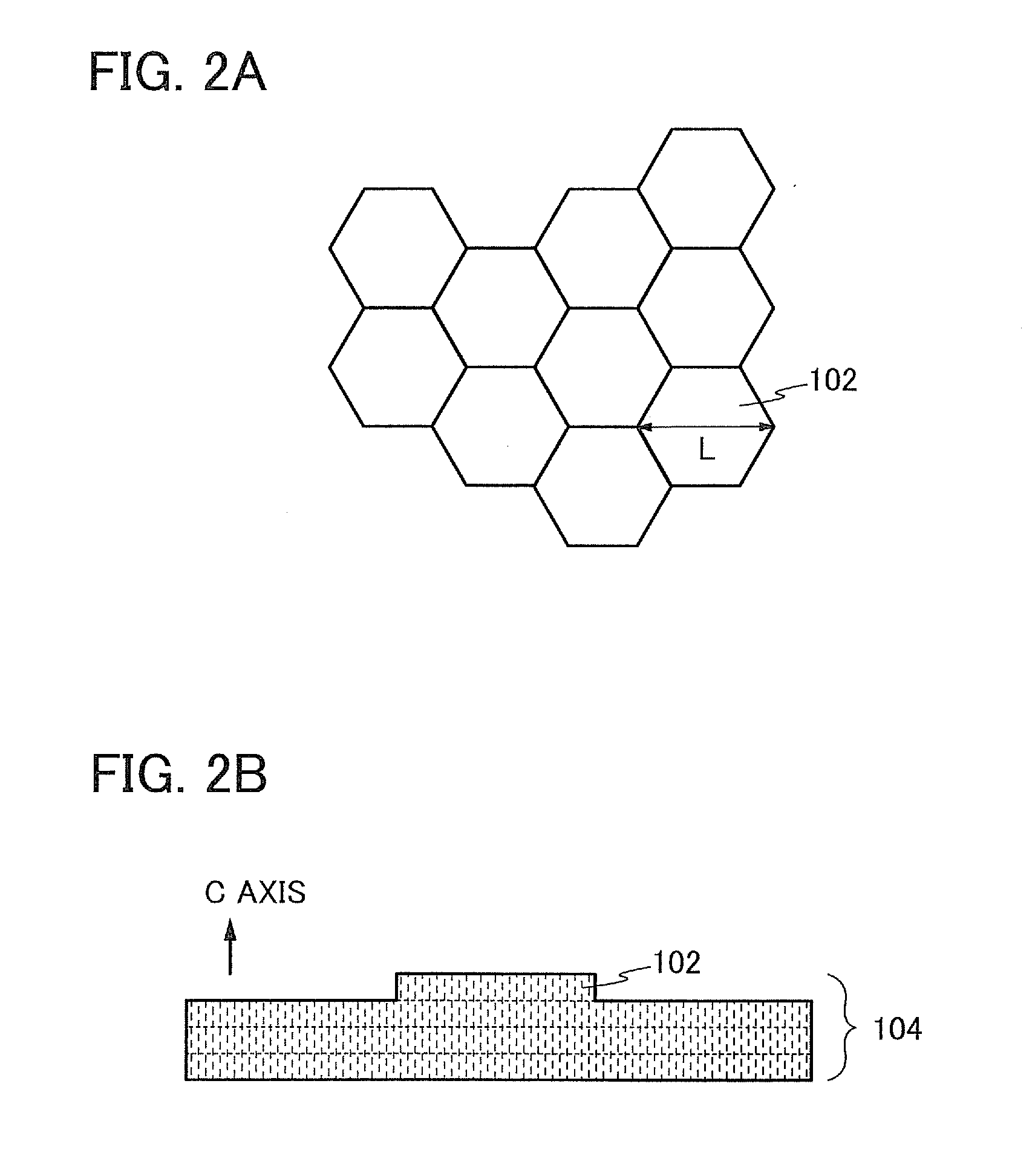
[0044]In this embodiment, a crystalline oxide semiconductor film according to one embodiment of the present invention and a film formation method thereof will be described with reference to FIG. 1, FIGS. 2A and 2B, FIGS. 3A and 3B, FIGS. 4A and 4B, and FIG. 5.

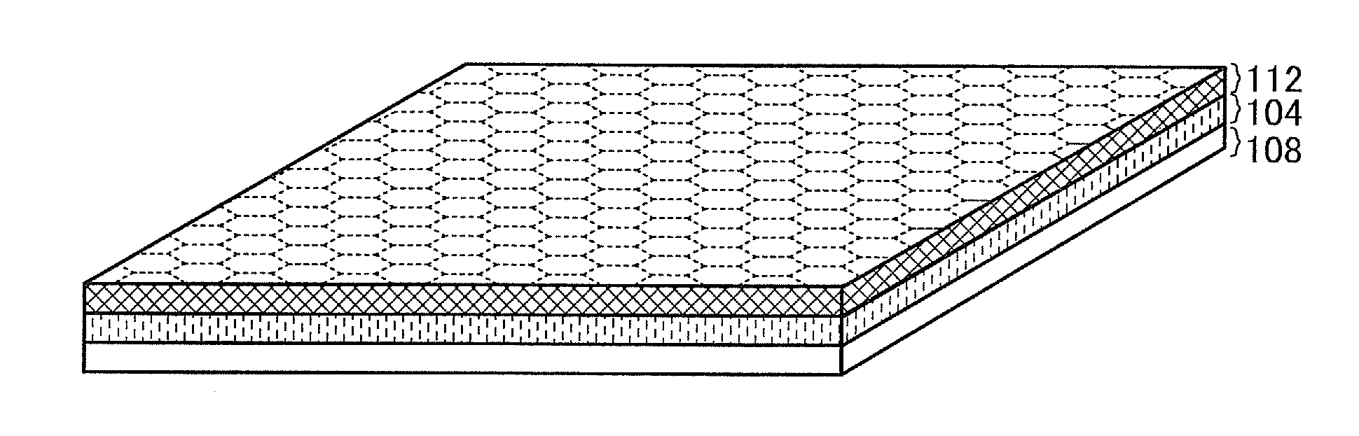
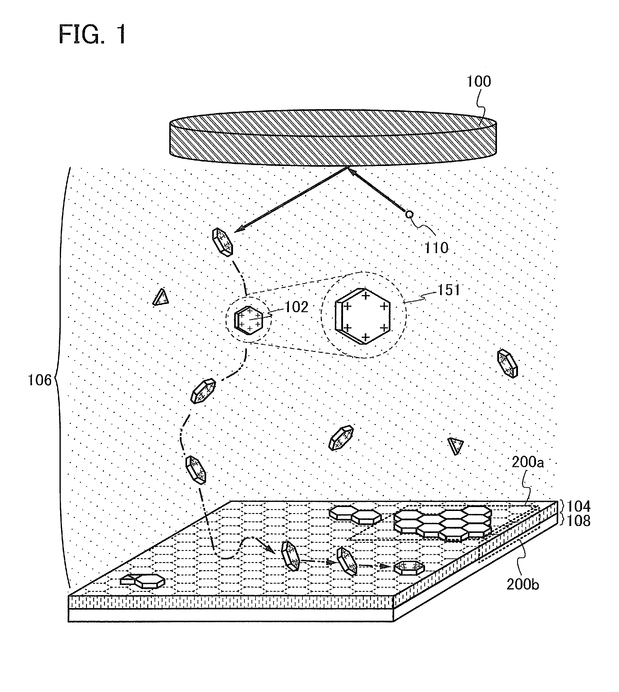
[0045]FIG. 1 is a schematic diagram illustrating a state in which an ion 110 collides with a sputtering target 100 to separate crystalline sputtered particles 102 from the sputtering target 100 and the crystalline sputtered particles 102 are transferred to a deposition surface (here, a surface of a base film 108).

[0046]Here, the sputtering target 100 includes a polycrystalline oxide containing a plurality of crystal grains each having a portion where an interatomic bond is weak in a plane parallel to an a-b plane.

[0047]For the sputtering target 100, a compound containing indium (In), gallium (Ga), zinc (Zn), and oxygen (O) can be used as a material, for example. Note that the plurality of crystal grains may have different grain...

embodiment 2

[0095]In this embodiment, a sputtering target which can be used for forming an oxide semiconductor film of one embodiment of the present invention will be described.

[0096]FIG. 6 shows an example of a fabrication process of a sputtering target.

[0097]First, raw materials are weighed and are mixed in a predetermined molar ratio (step S101).

[0098]In this embodiment, description is given on the case where an oxide powder containing In, m, and Zn (also referred to as an In-M-Zn oxide powder) is obtained as the oxide powder containing a plurality of metal elements.

[0099]Specifically, InOX oxide powder, MOY oxide powder, and ZnOZ powder are prepared and mixed in a predetermined molar ratio. Note that X, Y, and Z are each a given positive number; for example, X, Y, and Z are 1.5, 1.5, and 1, respectively.

[0100]It is needless to say that the above oxide powders are an example, and oxide powders can be selected as appropriate in order to obtain a desired composition. Note that Mrefers to Ga, S...

embodiment 3

[0117]In this embodiment, a structure example of a transistor to which the oxide semiconductor film including a single crystal region which is described in Embodiment 1 is applied will be described with reference to drawings. Note that the oxide semiconductor film formed by a sputtering method with the use of a sputtering target including a polycrystalline oxide containing a plurality of crystal grains is described in Embodiment 1; however, one embodiment of the present invention is not limited thereto. An oxide semiconductor film including a single crystal region which is formed without using a sputtering method can be used in some cases. Alternatively, an oxide semiconductor film including a single crystal region which is formed without using a sputtering target including a polycrystalline oxide containing a plurality of crystal grains can be used in some cases.

[0118]FIG. 7A illustrates a schematic cross-sectional view of a transistor 300. The transistor 300 exemplified by this st...


PUM

PropertyMeasurementUnit
temperatureaaaaaaaaaa
dew pointaaaaaaaaaa
dew pointaaaaaaaaaa

Abstract

An oxide semiconductor film with high crystallinity is formed. An oxide semiconductor film having a single crystal region, which is formed by a sputtering method using a sputtering target including a polycrystalline oxide containing a plurality of crystal grains, is provided. The plurality of crystal grains contained in the sputtering target has a plane that is cleaved or is likely to be cleaved because of a weak crystal bond; therefore, the cleavage planes in the plurality of crystal grains are cleaved when an ion collides with the sputtering target, whereby flat plate-like sputtered particles can be obtained. The obtained flat plate-like sputtered particles are deposited on a deposition surface; accordingly, an oxide semiconductor film is formed. The flat plate-like sputtered particle is formed by separation of part of the crystal grain and therefore the oxide semiconductor film can have high crystallinity.

Description

BACKGROUND OF THE INVENTION[0001]1. Field of the Invention[0002]The invention disclosed in this specification relates to an object, a method, a method for producing an object, a process, a machine, manufacture, or a composition of matter. In particular, the present invention relates to, for example, a semiconductor device, a display device, a light-emitting device, a driving method thereof, or a manufacturing method thereof. In particular, the present invention relates to, for example, an oxide semiconductor film included in a semiconductor device and a film formation method thereof.[0003]Note that a semiconductor device in this specification and the like refers to all types of devices which can function by utilizing semiconductor characteristics, and electro-optical devices, semiconductor circuits, and electronic devices are all semiconductor devices.[0004]2. Description of the Related Art[0005]A technique by which transistors are formed using semiconductor thin films formed over a...

Claims


Application Information

Patent Timeline
Patent Type & Authority Applications(United States)
IPC IPC(8): H01L29/22H01L21/02
Inventor YAMAZAKI, SHUNPEI
Owner SEMICON ENERGY LAB CO LTD
Why Eureka
Try Eureka