Resin composition with good workability, insulating film, and prepreg
a technology of insulating film and composition, which is applied in the direction of printed circuit details, printed circuit manufacturing, printed circuit aspects, etc., can solve the problems of increasing the functionality of printed circuit wiring, the inability to develop a high value-added prepreg, and the inability to work with a high-value-added prepreg, so as to increase the thermal and mechanical properties of an insulating material and maintain the workability.
- Summary
- Abstract
- Description
- Claims
- Application Information
AI Technical Summary
Benefits of technology
Problems solved by technology
Method used
Image
Examples
preparation example 1
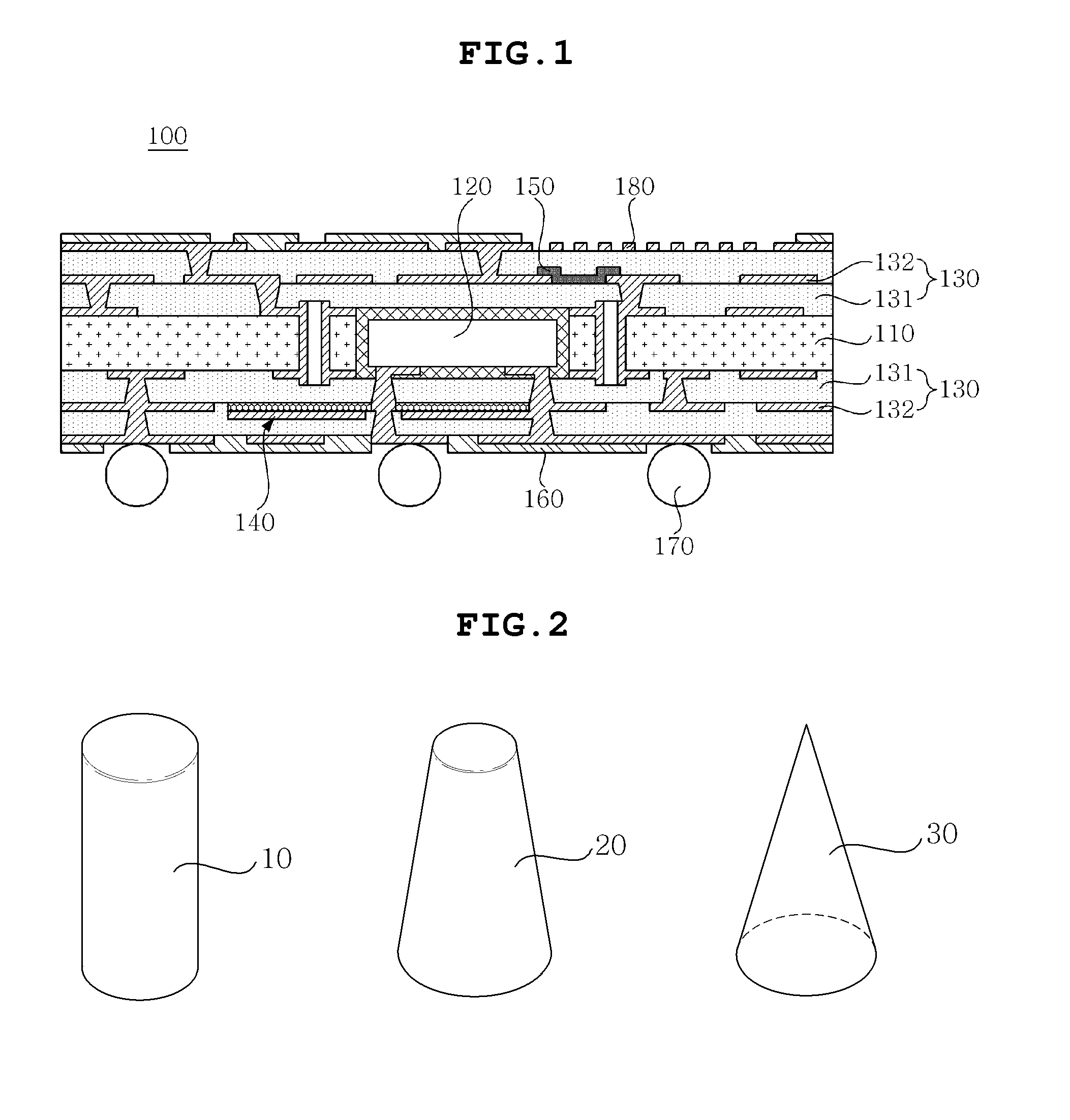
[0079]A p type silicon wafer was cut to a size of 1 cm×1 cm and then treated for 2 min in an aqueous hydrofluoric acid solution to remove silicon oxide from the wafer. The oxide-free silicon wafer was placed on the water surface of a beaker containing the aqueous solution of zinc nitrate hexahydrate (15 mM) and hexamethylenetetramine (15 mM) so that its surface was turned over. The aqueous solution was maintained at 93° C., and the total reaction time was 6 hr. Thereafter, the wafer was taken out of the aqueous solution, rinsed with water, and dried in air at 80° C. for 1 hr, thus manufacturing a zinc oxide nanorod (10 in FIG. 2).
[0081]The wafer having the zinc oxide nanorod was immersed in an aqueous hydrochloric acid solution having pH of 3 at room temperature, stirred for 30 min, and subjected to wet chemical etching. The wafer was removed from the aqueous hydrochloric acid solution, rinsed and then dried, thus obtaining a ...
example 1
[0082]Each of the zinc oxide nanorod and the zinc oxide nanocone of Preparation Example 1 in the amount shown in Table 1 below was mixed with 65 wt % of silica having an average diameter of 0.2˜1 μm in methylethylketone, and then added to an epoxy resin, Araldite MY-721 (Huntsmann), thus preparing a varnish. The varnish was applied to a thickness of 100 μm on the shiny surface of a copper foil using a doctor blade process, thus manufacturing a film. The film was dried at room temperature for 2 hr, dried in a vacuum oven at 80° C. for 1 hr, and then further dried at 110° C. for 1 hr, thus obtaining a semi-cured state (B-stage). This film was completely cured using a vacuum press. As such, the maximum temperature was 230° C. and the maximum pressure was 2 MPa. The CTE, Tg, and viscosity of the film were measured. The results are shown in Table 1 below.
[0083]Measurement of Thermal Properties
[0084]The CTE of the test sample of Example 1 was measured using a thermomechanical analyzer (TM...
PUM
| Property | Measurement | Unit |
|---|---|---|
| wt % | aaaaa | aaaaa |
| wt % | aaaaa | aaaaa |
| particle size | aaaaa | aaaaa |
Abstract
Description
Claims
Application Information


