Low void solder joint for multiple reflow applications

a solder joint and low void technology, applied in the field of low void solder joints for multiple reflow applications, can solve the problems of limiting the capacity of removing heat, the upper limit of these approaches is 5 w/m-k conductivity, and becoming a liability, so as to reduce the melting point and facilitate the spread of wetted surfaces

Active Publication Date: 2014-07-10
INDIUM CORP
View PDF2 Cites 16 Cited by
  • Summary
  • Abstract
  • Description
  • Claims
  • Application Information

AI Technical Summary

Benefits of technology

[0018]The combination of formic acid fluxless soldering and the use of silver as the metallization enable this process. Silver forms a eutectic alloy with indium at a level of 3% indium. When liquid indium from the solder TIM contacts the silver it immediately wets and quickly dissolves the silver. In this application, the leaching of the silver allows the indium to solder to the underlying nickel. The In—Ni solder joint is very stable with a slow-growing intermetallic layer.
[0020]For the multiple reflow application, the silver metallization on the heat spreader plays the role of a reservoir of filler for the bond line. The liquid indium in contact with silver initially seeks to form the In—Ag IMC. This is quickly dissolved in the indium, lowering its melting point to from 157° C. to the In—Ag eutectic of 143° C. This low melting eutectic assists the spreading of the wetted surface providing a mobile source of liquid solder during each melting cycle.

Problems solved by technology

With the progression of more BGA (ball grid array) packages in circuits, there is a problem with the conventional indium solder processes that use a liquid flux as well as with interfaces that are created using a polymer based thermal interface material (TIM) such as a phase change material, gel, thermal grease or polymer solder hybrid.
In the case of epoxies, greases and gels, the low thermal conductivity of the polymer limits its capacity for removing heat.
However, the upper limit of these approaches is ˜5 W / m-K conductivity.
This becomes a liability when the interface gap prevents forming a uniform and thin bond line.
These interfaces often flex and bow considerably during the thermal cycles of processing as well as during service.
However, polymer-based TIMs mechanically adhere to each interface rather than form a physical and chemical bond like a solder does as intermetallics.
In the case of polymer-based TIMs, subsequent reflows also deteriorate the TIM by hardening the polymers, as well as causing bake out of the TIM, or outgassing, which in turn increases thermal resistance of the interface.
When this solder joint is created with a liquid flux, it will have some voids, and those voids often contain liquid flux residue.
When this liquid flux created solder joint goes through subsequent reflows either at the original reflow temperature or elevated temperature, the flux residue is baked and volatized, which in most cases causes bigger voids and void propagation.
Voids are significantly less thermally and electrically conductive than metallic solder and impair the efficiency and quality of the TIM.
Liquid flux is also an issue because liquid flux materials are likely corrosive unless it is cleaned after reflow.
However, the vacuum processes often have manufacturing throughput limitations as small batches of components are loaded in the chamber and evacuated, heated, flowed and cooled.

Method used


Image

  • Low void solder joint for multiple reflow applications
  • Low void solder joint for multiple reflow applications
  • Low void solder joint for multiple reflow applications

Examples


Embodiment Construction

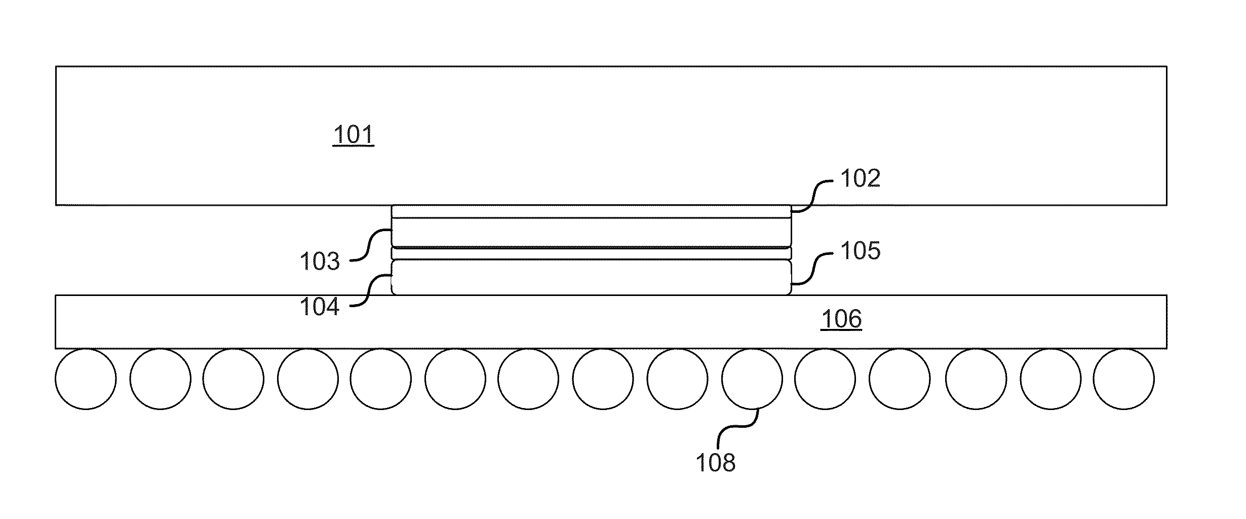
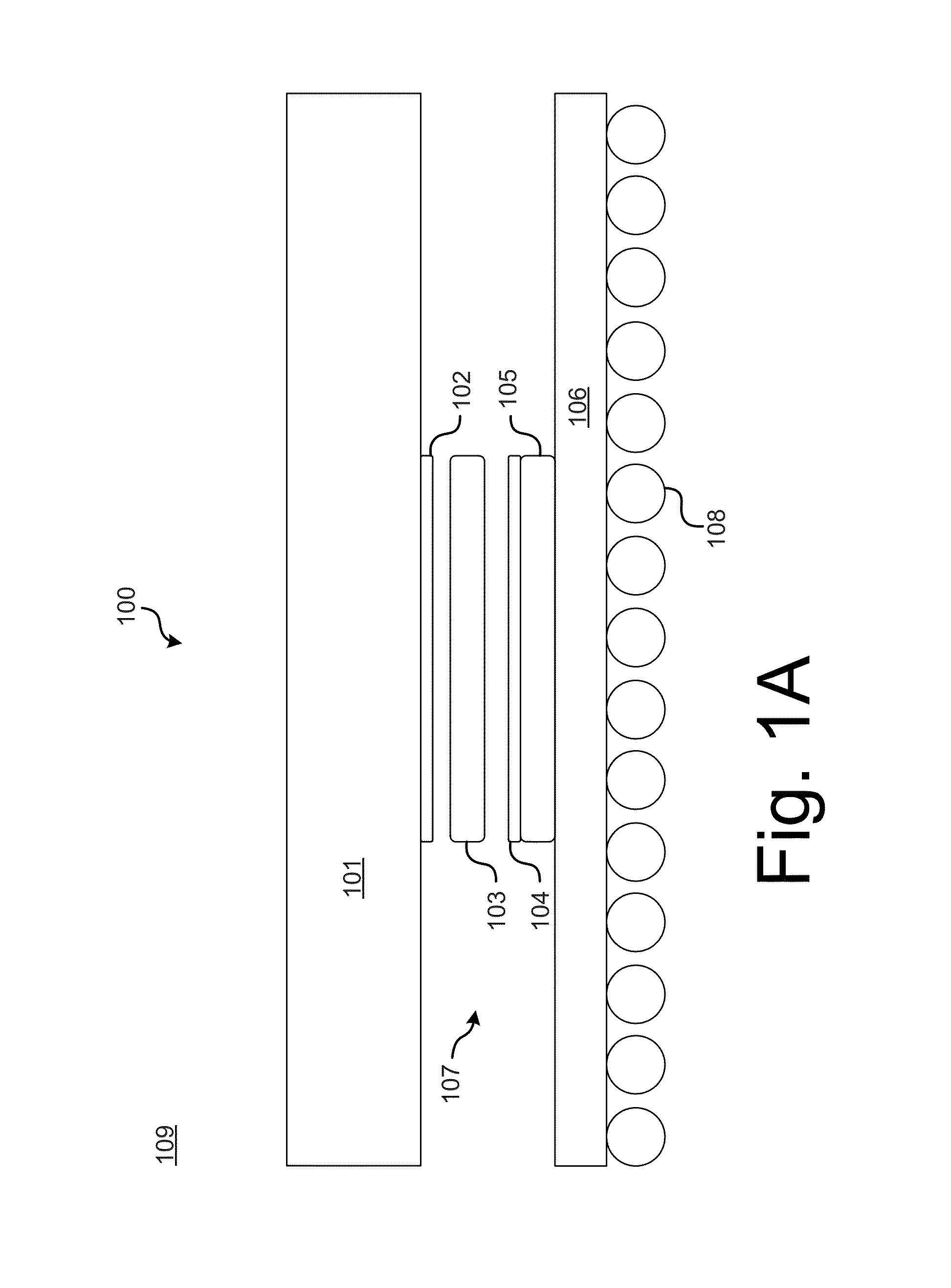
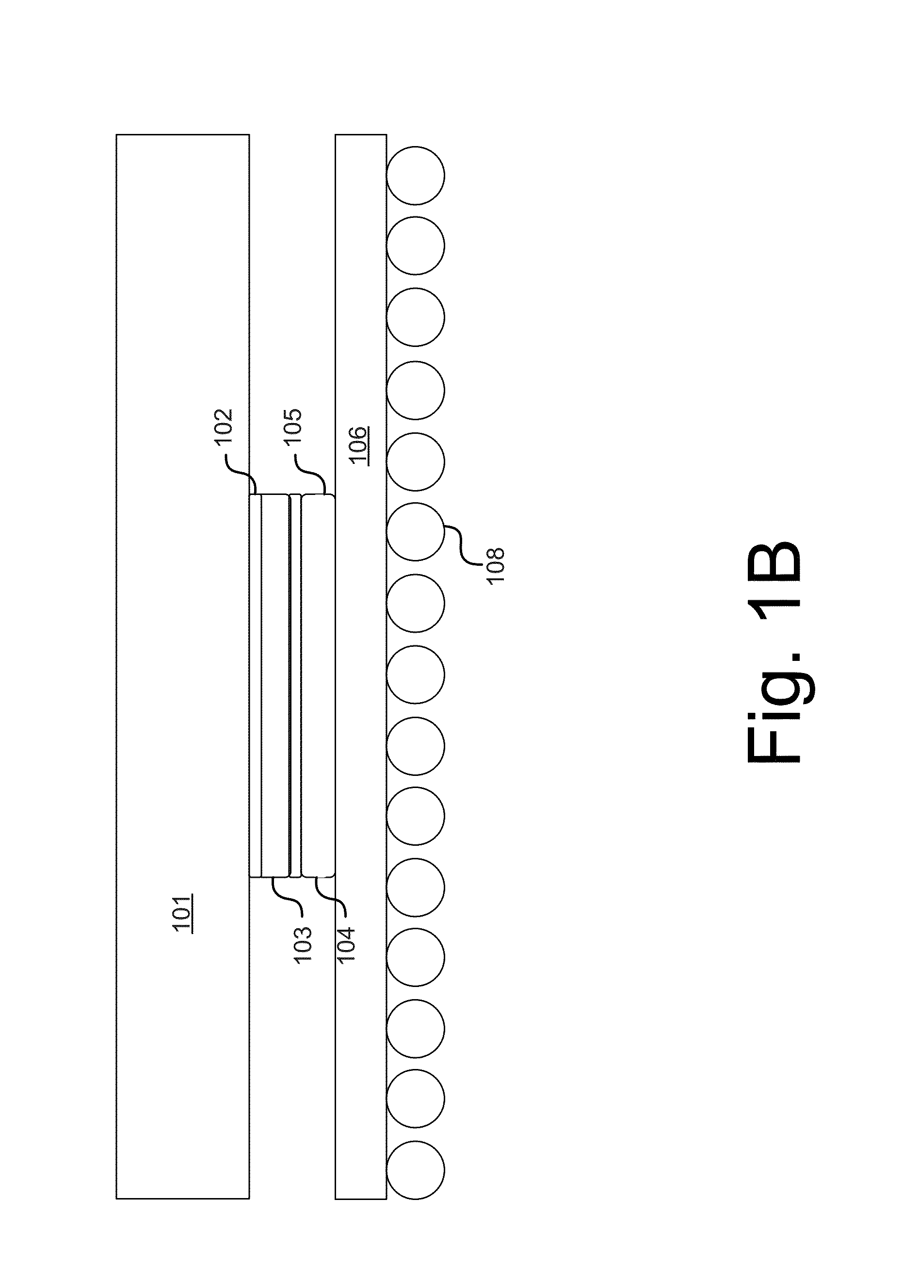
[0017]Embodiments of the technology disclosed herein use fluxless soldering in an in-line oven, which forms a robust solder thermal interface capable of remaining essentially void-free through multiple reflow cycles. This technology can use a sacrificial silver metallization rather than gold. The result is a solder joint bonded directly to the underlying nickel without the brittle layer of an In2Au intermetallic compound.

[0018]The combination of formic acid fluxless soldering and the use of silver as the metallization enable this process. Silver forms a eutectic alloy with indium at a level of 3% indium. When liquid indium from the solder TIM contacts the silver it immediately wets and quickly dissolves the silver. In this application, the leaching of the silver allows the indium to solder to the underlying nickel. The In—Ni solder joint is very stable with a slow-growing intermetallic layer.

[0019]This type of reaction also occurs in the gold metallized interface; except that indium...


PUM

PropertyMeasurementUnit
melting pointaaaaaaaaaa
melting temperaturesaaaaaaaaaa

Abstract

Methods and apparatus are provided for attaching a heat spreader to a die and includes disposing a solder thermal interface material between a first surface of a die and a first surface of a heat spreader without disposing a liquid flux between the die and the heat spreader to form an assembly, wherein at least one of the first surface of the die and a first surface of the heat spreader have disposed thereon a metallization structure comprising a transition layer and a sacrificial metallization layer, the sacrificial metallization layer disposed as an outer layer to the metallization structure adjacent the solder thermal interface material; and heating the assembly to melt the thermal interface and attach the die to the heat spreader.

Description

CROSS-REFERENCE TO RELATED APPLICATIONS[0001]This application is a continuation of and claims the benefit of U.S. patent application Ser. No. 13 / 483,376, filed May 30, 2012.TECHNICAL FIELD [0002]The present invention relates generally to solder applications, and more particularly soldering without a liquid flux, some embodiments relate to creation of solder joints with low voiding suitable for multiple reflow processes.DESCRIPTION OF THE RELATED ART [0003]Components such as microprocessors, power amplifiers, microwave generators and similar semiconductor devices, generate considerable ohmic heating while performing the computing or controlling functions. This heating must be removed efficiently at relatively low temperatures to prevent break-down of the semi-conductor circuitry. Although a number of different methods are employed to draw the heat from the semiconducting die, the most effective is achieved by direct conduction through a flat face of the die. In the case of a typical ...

Claims


Application Information

Patent Timeline
Patent Type & Authority Applications(United States)
IPC IPC(8): H05K13/04
CPCH05K13/0465H01L24/83H01L2924/15311H01L23/36H01L23/3736H01L2924/01327H01L2224/29012H01L2224/27334H01L23/10H01L21/50H01L24/16H01L24/27H01L24/29H01L24/32H01L24/73H01L24/81H01L24/92H01L2224/16225H01L2224/29015H01L2224/29018H01L2224/29109H01L2224/32225H01L2224/32245H01L2224/73204H01L2224/73253H01L2224/81815H01L2224/83001H01L2224/83075H01L2224/83136H01L2224/8314H01L2224/8321H01L2224/83439H01L2224/83444H01L2224/83447H01L2224/83455H01L2224/83815H01L2224/92125H01L2224/92225H01L2224/2711H01L2224/29016H01L2924/01322H01L2924/00011Y10T428/12222H01L2924/00H01L2924/00012H01L2224/83205
Inventor ROSS, JORDAN PETERHARTNETT, AMANDAJARRETT, ROBERT NORMAN
Owner INDIUM CORP
Why Eureka
Try Eureka