One-dimensional conductive nanomaterial-based conductive film having the conductivity thereof enhanced by a two-dimensional nanomaterial

a technology of conductive nanomaterials and conductive films, which is applied in the direction of conductive layers on insulating supports, applications, conductors, etc., can solve the problems of unstable supply and demand of indium oxide (in2o3), high production costs, and deterioration of electrical conductivity of indium oxide, so as to enhance the conductivity of one-dimensional conductive nanomaterial films

Inactive Publication Date: 2014-07-31
KOREA ELECTROTECH RES INST
View PDF5 Cites 21 Cited by
  • Summary
  • Abstract
  • Description
  • Claims
  • Application Information

AI Technical Summary

Benefits of technology

[0020]Accordingly, there is an advantage of enhancing the conductivity of a one-dimensional conductive nanomaterial film by laminating a two-dimensional nanomaterial, such as graphene or the like, on the upper surface of a film composed of a one-dimensional conductive nanomaterial such as carbon nanotubes, metal nanowires, metal nanorods or the like.
[0021]According to the present invention, there is an effect of enhancing the conductivity of a one-dimensional conductive nanomaterial film by laminating a two-dimensional nanomaterial, such as graphene or the like, on the upper surface of a film composed of a one-dimensional conductive nanomaterial such as carbon nanotubes, metal nanowires, metal nanorods or the like.

Problems solved by technology

The ITO film is advantageous in that it has excellent physical properties, and, to date, it has frequently been introduced in processes, but is problematic in that the supply and demand of indium oxide (In2O3) is unstable because indium oxide (In2O3) is produced as a by-product from a zinc (Zn) mine or the like.
Further, the ITO film is problematic in that it cannot be used for a flexible substrate, such as a polymer substrate or the like, because it does not have flexibility, and in that its production cost is high because it must be prepared at high-temperature and high-pressure conditions.
However, such a flexible conductive film is problematic in that its electrical conductivity is deteriorated when it is exposed to an external environment, and it is not transparent, thus restricting the use thereof.
This conventional technology is problematic in that only carbon nanotubes having an outer diameter of 3.5 nm can be used in consideration of dispersibility and electrical conductivity, and thus the usage thereof is restricted, and in that the dispersibility and adhesivity of carbon nanotubes are deteriorated at the time of forming a coating film, and thus the characteristics of the coating film are deteriorated with the passage of time.
This conventional technology is also problematic in that the packing density of a carbon nanotube network is not high, so junction resistance increases, thereby decreasing conductivity, and in that carbon nanotubes have hydrophobicity, and thus it is difficult to apply a hydrophilic material onto carbon nanotubes.
Further, this conventional technology is problematic in that carbon nanotubes have pores on the surface thereof, so the surface thereof becomes rough, and thus there is a limitation in using carbon nanotubes as photoelectric elements.

Method used


Image

  • One-dimensional conductive nanomaterial-based conductive film having the conductivity thereof enhanced by a two-dimensional nanomaterial
  • One-dimensional conductive nanomaterial-based conductive film having the conductivity thereof enhanced by a two-dimensional nanomaterial
  • One-dimensional conductive nanomaterial-based conductive film having the conductivity thereof enhanced by a two-dimensional nanomaterial

Examples


first embodiment

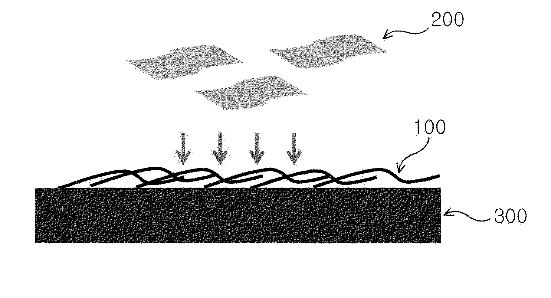
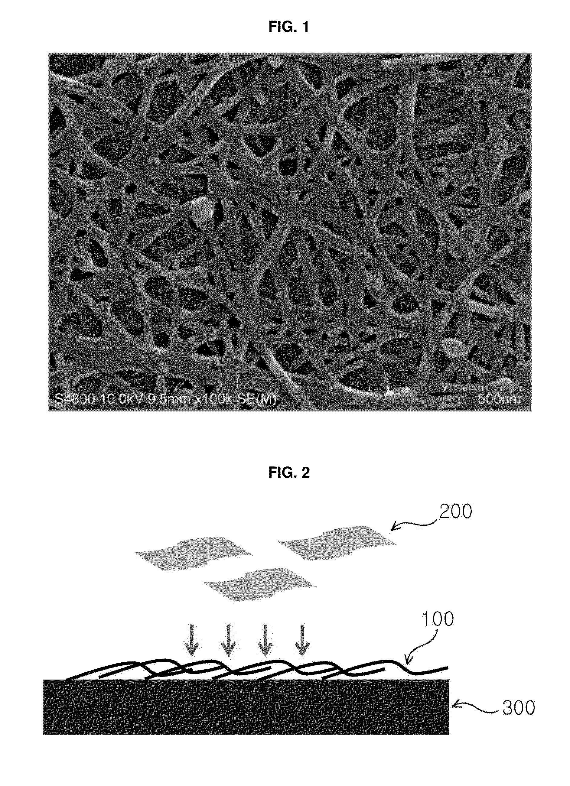
[0033]First, a one-dimensional conductive nanomaterial layer will be described.

[0034]The one-dimensional conductive nanomaterial layer is formed on a plastic substrate using a one-dimensional conductive nanomaterial. In this embodiment, as the substrate, a polyethylene terephthalate substrate is used. Further, as the one-dimensional conductive nanomaterial, carbon nanotubes, metal nanowires, metal nanorods or the like may be used, but, in this embodiment, carbon nanotubes are used.

[0035]First, 1 mg of single-wall carbon nanotubes are added to 100 mL of a surfactant solution (concentration: 1%), the carbon nanotubes are dispersed for 1 hour using a sonicator, and then the surfactant solution dispersed with carbon nanotubes is treated by a centrifugal separator at a rotation speed of 100 rpm for 30 min to separate upper-layer liquid, thereby preparing a carbon nanotube solution.

[0036]Subsequently, the prepared carbon nanotube solution is applied onto a polyethylene terephthalate subst...

second embodiment

[0055]In second embodiment of the present invention, a carbon nanotube transparent conductive film was formed in the same manner as in first embodiment, except that boron nitride was used as a two-dimensional nanomaterial.

[0056]Boron nitride, similarly to graphite, is structured such that two-dimensional boron nitride layers are piled in layers.

[0057]In this embodiment, boron nitride was dispersed in an organic solvent such as alcohol or the like, and then treated with a sonicator and a homogenizer to prepare a two-dimensional boron nitride coating solution, and then the two-dimensional boron nitride coating solution is formed into a boron nitride sheet.

[0058]FIG. 10 is a scanning electron microscope photograph of the formed two-dimensional boron nitride sheet. From FIG. 10, it can be ascertained that two-dimensional boron nitride sheet is a single layer.

[0059]The prepared boron nitride coating solution was applied onto a carbon nanotube transparent conductive film to form a two-dim...


PUM

PropertyMeasurementUnit
outer diameteraaaaaaaaaa
water contact angleaaaaaaaaaa

Abstract

A one-dimensional conductive nanomaterial-based conductive film having the conductivity thereof enhanced by a two-dimensional nanomaterial in which the conductive film includes a substrate, a one-dimensional conductive nanomaterial layer formed on the substrate, and a two-dimensional nanomaterial layer formed on the one-dimensional conductive nanomaterial layer, wherein the one-dimensional conductive nanomaterial layer includes a one-dimensional conductive nanomaterial formed of at least one selected from a carbon nanotube, a metal nanowire, and a metal nanorod, and the two-dimensional nanomaterial layer includes a two-dimensional nanomaterial formed of at least one selected from graphene, boron nitride, tungsten oxide (WO3), molybdenum sulfide (MoS2), molybdenum telluride (MoTe2), niobium diselenide (NbSe2), tantalum diselenide (TaSe2), and manganese dioxide (MnO2). A two-dimensional nanomaterial, such as graphene may be stacked on a one-dimensional conductive nanomaterial such as a carbon nanotube or a metal nanowire to enhance the conductivity of the one-dimensional conductive nanomaterial film.

Description

REFERENCE TO RELATED APPLICATIONS[0001]This is a continuation of pending International Patent Application PCT / KR2011 / 009444 filed on Dec. 8, 2011, which designates the United States and claims the priority benefit of Korean Patent Application No. 10-2011-0101907 filed on Oct. 6, 2011, the entire contents of which are incorporated herein by reference.FIELD OF THE INVENTION[0002]The present invention relates to a one-dimensional conductive nanomaterial-based conductive film having conductivity thereof enhanced by a two-dimensional nanomaterial. More particularly, the present invention relates to a one-dimensional conductive nanomaterial-based conductive film, wherein the conductivity thereof is enhanced by laminating a two-dimensional nanomaterial, such as graphene or the like, on the upper surface of a film composed of a one-dimensional conductive nanomaterial such as carbon nanotubes, metal nanowires or the like.BACKGROUND OF THE INVENTION[0003]Generally, a transparent conductive fi...

Claims


Application Information

Patent Timeline
Patent Type & Authority Applications(United States)
IPC IPC(8): H01B1/24H01B1/22C09D7/61C09D7/62
CPCH01B1/22H01B1/24B82Y30/00H01L31/022466H01L31/1884C09D11/52Y02E10/549C09D5/24C08K3/04C08K3/08C09D7/70Y10T428/30C09D7/62C09D7/61H10K30/821H01B1/00H01B5/14
Inventor HAN, JOONG-TARKLEE, GEON-WOONGJEONG, HEE-JINJEONG, SEUNG-YOLKIM, JUN-SUK
Owner KOREA ELECTROTECH RES INST
Why Eureka
Try Eureka