Thin film transistor, method of manufacturing the same, and image display device equipped with thin film transistor

a thin film transistor and manufacturing method technology, applied in the direction of semiconductor devices, instruments, electrical appliances, etc., can solve the problems of difficult work, low resistance to aging, and difficult film work, and achieve the effect of simple manufacturing process, low cost and high quality

Inactive Publication Date: 2014-08-07
TOPPAN PRINTING CO LTD
View PDF3 Cites 29 Cited by
  • Summary
  • Abstract
  • Description
  • Claims
  • Application Information

AI Technical Summary

Benefits of technology

[0029]According to the invention recited in claim 1 of the present invention, a bottom-gate thin film transistor based on a metal oxide semiconductor enables a patterning process of the metal oxide layer, i.e. a wet etching process, to be eliminated. This makes it possible to simplify the manufacturing processes of the thin film transistor.
[0030]This provides the thin film transistor manufacturable in high quality and low cost and the method of manufacturing the thin film transistor, and an image display device equipped with the thin film transistor.
[0031]According to the invention recited in claim 2 of the present invention, the electric conductivity of the semiconductor region fog ivied on the first gate insulating layer as the metal oxide layer is higher than that of the insulating layer formed on the second gate insulating layer as the metal oxide layer.
[0032]Note that the present invention is based on the fact that changing the composition in the film enables the electric conductivity of a metal oxide layer to be easily controlled. If a gate insulating layer, which serves as a foundation layer for the metal oxide layer, contains hydrogen atoms, the hydrogen atoms diffuse from the gate insulating layer into the metal oxide layer, and the diffused hydrogen atoms act as donors. This increases the electric conductivity.
[0033]The concentration of hydrogen atoms in each of the first gate insulating layer and the second gate insulating layer is changed. This change permits, during deposition of the metal oxide layer constituting the thin film transistor, the semiconductor region and the insulating region to be simultaneously formed respectively on the gate insulating layer with the high concentration of hydrogen atoms and on the gate insulating layer with the low concentration of hydrogen atoms. That is, the semiconductor region has a high conductivity and shows semiconductor characteristics, and the insulating region has a low conductivity and shows insulating characteristics. This results in elimination of a patterning process of the semiconductor layer.
[0034]According to the invention recited in claim 5 of the present invention, the electric conductivity of the metal oxide layer formed below the first insulating protective layer is higher than that of the metal oxide layer formed below the second insulating protective layer.

Problems solved by technology

For this reason, in order to fabricate flexible devices, very expensive, high water-absorption films, i.e. films that are difficult to work with, including high thermal-resistance polyimide films must be used as their substrates.
However, the organic semiconductor materials have a very low mobility, and a low resistance to aging, so they have not been widely used.

Method used


Image

  • Thin film transistor, method of manufacturing the same, and image display device equipped with thin film transistor
  • Thin film transistor, method of manufacturing the same, and image display device equipped with thin film transistor
  • Thin film transistor, method of manufacturing the same, and image display device equipped with thin film transistor

Examples


examples

[0222]Examples of the present invention will be described hereinafter using comparative examples.

first embodiment

Examples of the First Embodiment

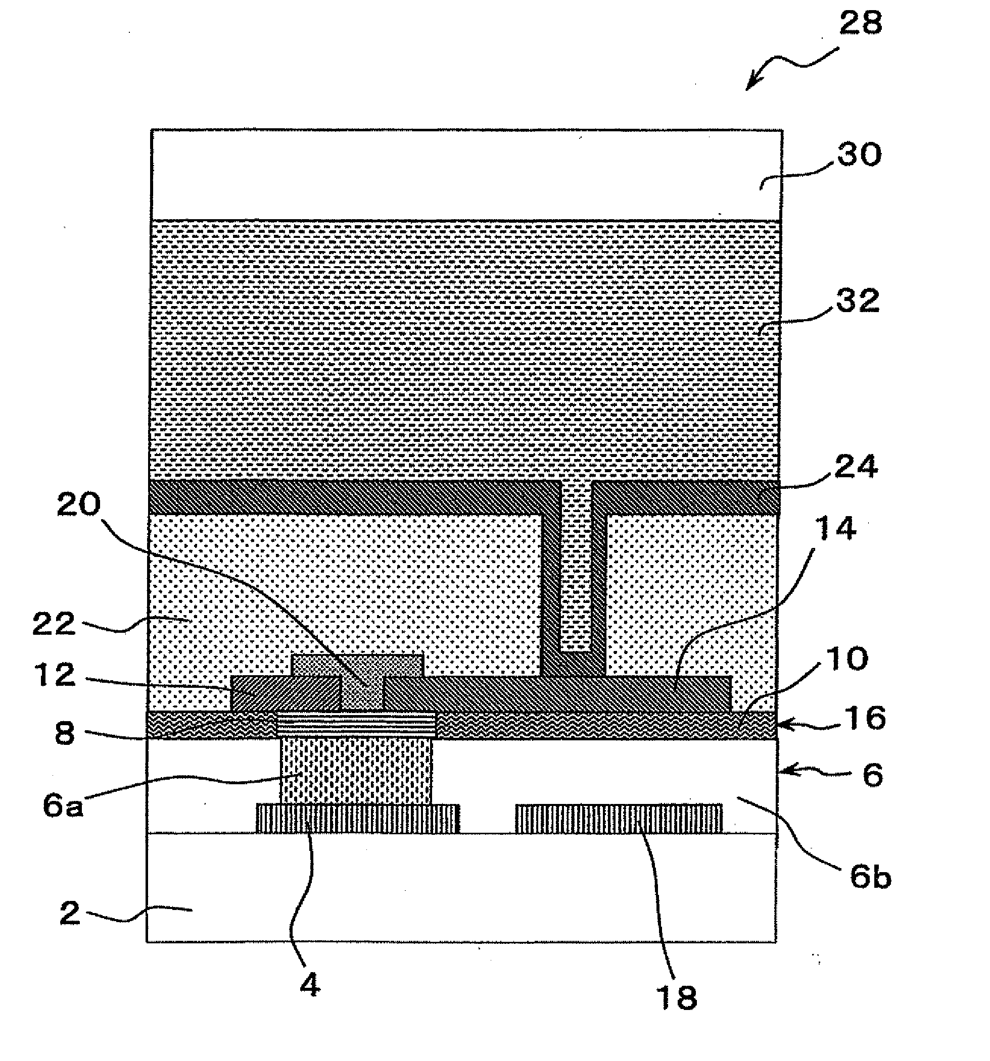
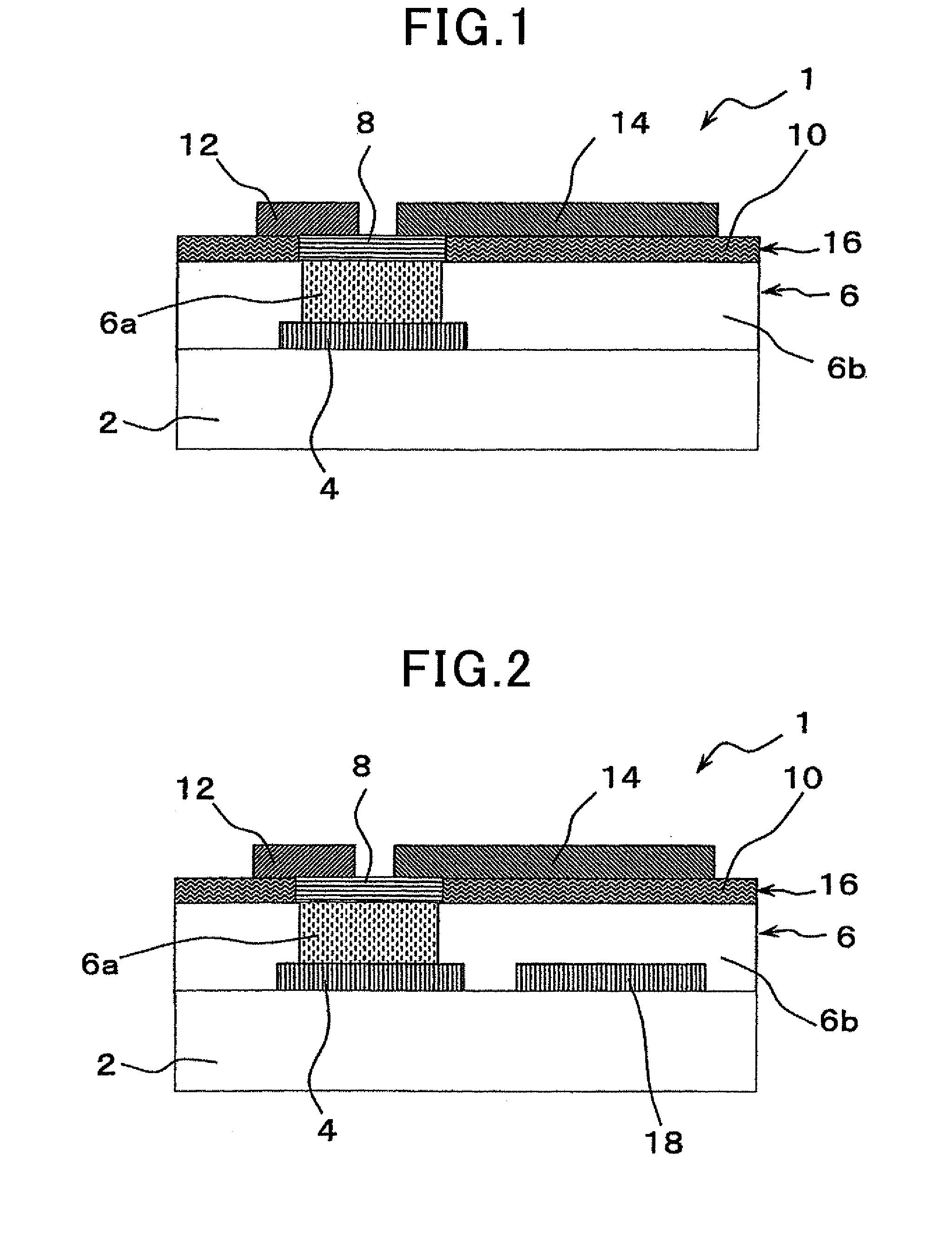
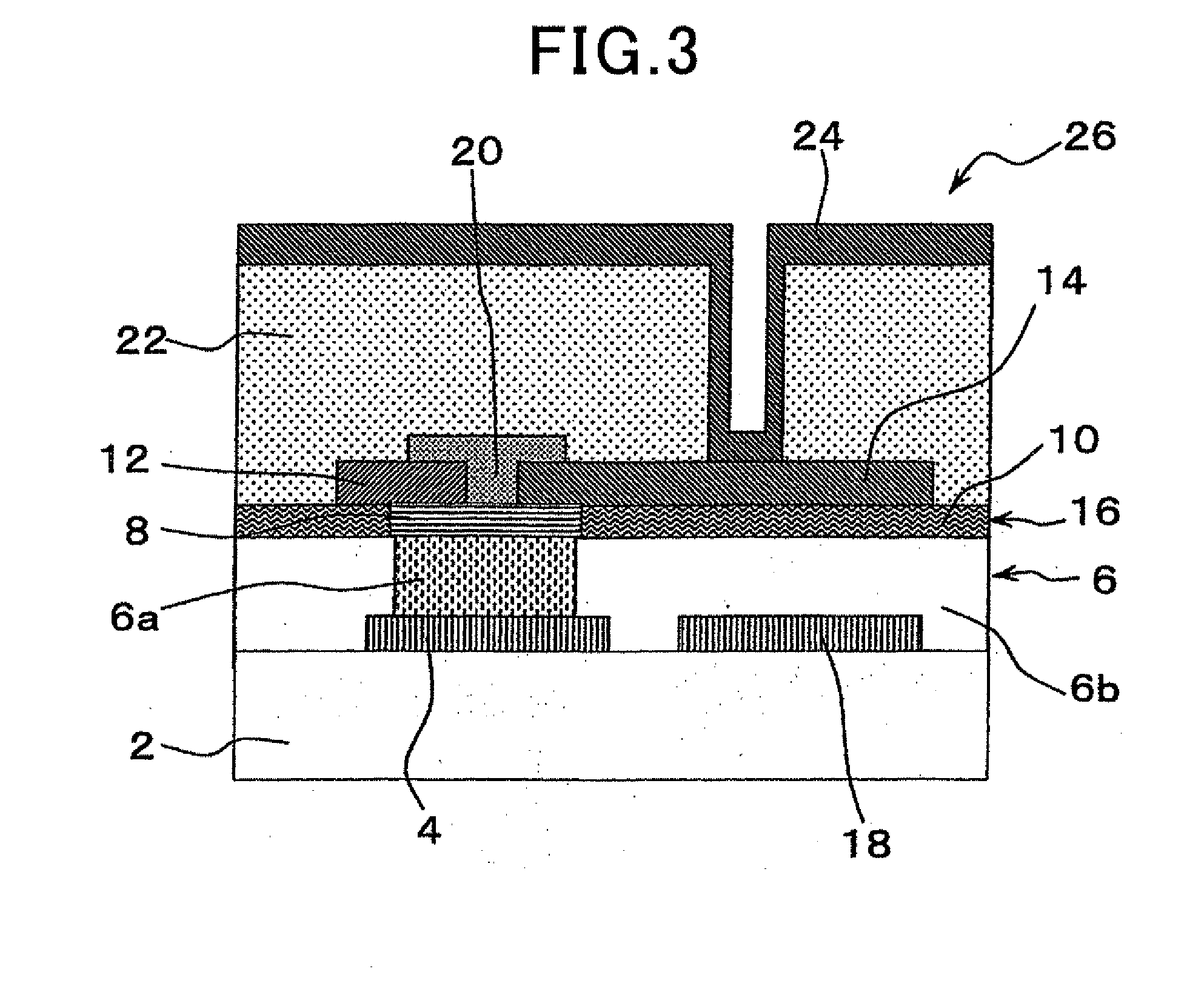
[0223]Three types of thin film transistors 1 according to the first embodiment were manufactured, three types of thin film transistors 1 according to the comparative examples were manufactured, and the physical properties of each of these manufactured thin film transistors 1 were evaluated based on FIGS. 2 to 5 in reference to FIG. 1. The results of the physical property evaluation will be described hereinafter.

first example

[0224]The thin film transistor 1, i.e. the thin film transistor element, illustrated in FIG. 2 was manufactured as the thin film transistor 1 according to the first example. Note that FIG. 2 is a cross sectional view of schematically illustrating the thin film transistor 1 according to this example.

[0225]In manufacturing the thin film transistor 1 according to the first example, an Mo film was deposited to have a thickness of 80 nm on a PEN substrate with a thickness of 125 μm at room temperature using a DC magnetron sputtering system.

[0226]Next, after formation of a resist pattern using photolithography, dry etching and stripping were performed, so that the gate electrode 4 and a capacitor electrode 18 were formed.

[0227]At that time, input power, gas flow rate Ar, and deposition pressure during Mo-film formation were set to 100 W, 50 SCCM, and 1.0 Pa, respectively.

[0228]Next, an SiNx film was deposited to have a thickness of 500 nm using a plasma CVD system. After formation of a re...


PUM


Abstract

A thin film transistor includes, on an insulating substrate, at least: a gate electrode; a gate insulating layer; a source electrode; a drain electrode; a metal oxide layer including a semiconductor region and an insulating region, each of the semiconductor region and the insulating region being composed of a same metal oxide material; and an insulating protective layer. The semiconductor region includes a region between the source electrode and the drain electrode, and is overlaid on a part of each of them. The semiconductor region is formed between the gate insulating layer and the insulating protective layer to abut on at least one of them. The electric conductivity of the semiconductor region is higher than that of the insulating region.

Description

TECHNICAL FIELD[0001]The present disclosure relates to thin film transistors, methods of manufacturing thin film transistors, and image display devices equipped with thin film transistors.BACKGROUND ART[0002]Active-matrix FPDs (Flat Panel Displays), which are driven by thin film transistors with amorphous-silicon or polycrystalline-silicon channel layers, are the mainstream of general FPDs.[0003]Production of high-quality amorphous silicon or polycrystalline silicon requires high deposition temperatures of 300° C. or thereabout. For this reason, in order to fabricate flexible devices, very expensive, high water-absorption films, i.e. films that are difficult to work with, including high thermal-resistance polyimide films must be used as their substrates.[0004]In recent years, thin film transistors using organic semiconductor materials have been studied actively.[0005]Because such organic semiconductor materials can be produced in a printing process without using a vacuum process, th...

Claims


Application Information

Patent Timeline
Patent Type & Authority Applications(United States)
IPC IPC(8): H01L29/786H01L29/66
CPCH01L29/66742H01L29/7869H01L27/1225H01L29/4908H01L29/66969H01L29/78606G02F1/167H01L29/51
Inventor IMAMURA, CHIHIROMIYAIRI, YUKARIKOYAMA, HIROAKI
Owner TOPPAN PRINTING CO LTD
Why Eureka
Try Eureka