Method of making cavity substrate with built-in stiffener and cavity substrate manufactured thereby

a technology of cavity substrate and built-in stiffener, which is applied in the direction of printed circuit manufacturing, semiconductor/solid-state device details, printed circuit aspects, etc., can solve the problems of increasing the thickness of the metal block, reducing the diameter of the metal block in order to increase the wiring density, and prone to warpage problems, etc., to achieve high manufacturing yield, easy manufacturing process, and low coefficient of thermal expansion

Inactive Publication Date: 2014-09-04
BRIDGE SEMICON
View PDF2 Cites 37 Cited by
  • Summary
  • Abstract
  • Description
  • Claims
  • Application Information

AI Technical Summary

Benefits of technology

[0039]The present invention also provides a semiconductor assembly in which a semiconductor device can extend into the cavity defined in the adhesive and be electrically connected to the conductive via or the circuitry layer exposed from the cavity using a wide variety of connection media including gold or solder bumps or bonding wires. Optionally, an under-fill can be dispensed within the cavity and a heat sink may be attached on the semiconductor device to enhance thermal performance.
[0044]The present invention has numerous advantages. The supporting board which contains a stiffener provides a flat and stable platform for attaching the interconnect substrate and thus make the manufacturing process easy to handle. The bump of the sacrificial carrier which defines a cavity area for device placement can only be separated from the dielectric layer by etching thus ensure a high manufacturing yield without un-predictable peeling or delamination concern. Furthermore, vast options of the built-in stiffener ranging from low coefficient of thermal expansion (CTE) materials like ceramics, to high thermal conductive materials like metal plate, to low cost materials like glass-fiber epoxy provide diversified solutions for various packaging designs. As a result, a semiconductor device can be mounted into the cavity without special alignment tool to achieve low profile and small form-factor requirements. The electrical connection between the semiconductor device and the interconnect substrate can be successfully established through the well-defined conductive vias or the exposed portion of the circuitry layer at the cavity without the troublesome matter that the lamination-induced displacement and warping which often cause the failure of semiconductoor package. The plated through-hole can provide vertical signal routing between the interconnect substrate and the terminal, thereby providing the cavity substrate with stacking capability.

Problems solved by technology

As plated-through-hole in the copper-clad laminate core is typically formed by mechanical CNC drill, reducing its diameter in order to increase wiring density may encounter seriously technical limitations and often very costly.
However, as coreless boards do not have a core layer to provide a necessary flexural rigidity, they are more susceptible to warpage problem when under thermal stress compared to that of conventional boards with core layers.
In this approach, although a supporting platform can be created and warping issues may be improved, etching a thick metal block is prohibitively cumbersome, low throughput, and prone to create many yield-loss issues such as an uncontrollable boundary line due to etching under-cut.
Since the peeling promotion layer, either a thermal setting resin or an oxide film, has the peeling off property when under a heat or light treatment, there exists a high risk of early delamination during dielectric layer coating and curing, this may result in serious yield and reliability concerns.

Method used


Image

  • Method of making cavity substrate with built-in stiffener and cavity substrate manufactured thereby
  • Method of making cavity substrate with built-in stiffener and cavity substrate manufactured thereby
  • Method of making cavity substrate with built-in stiffener and cavity substrate manufactured thereby

Examples


embodiment 1

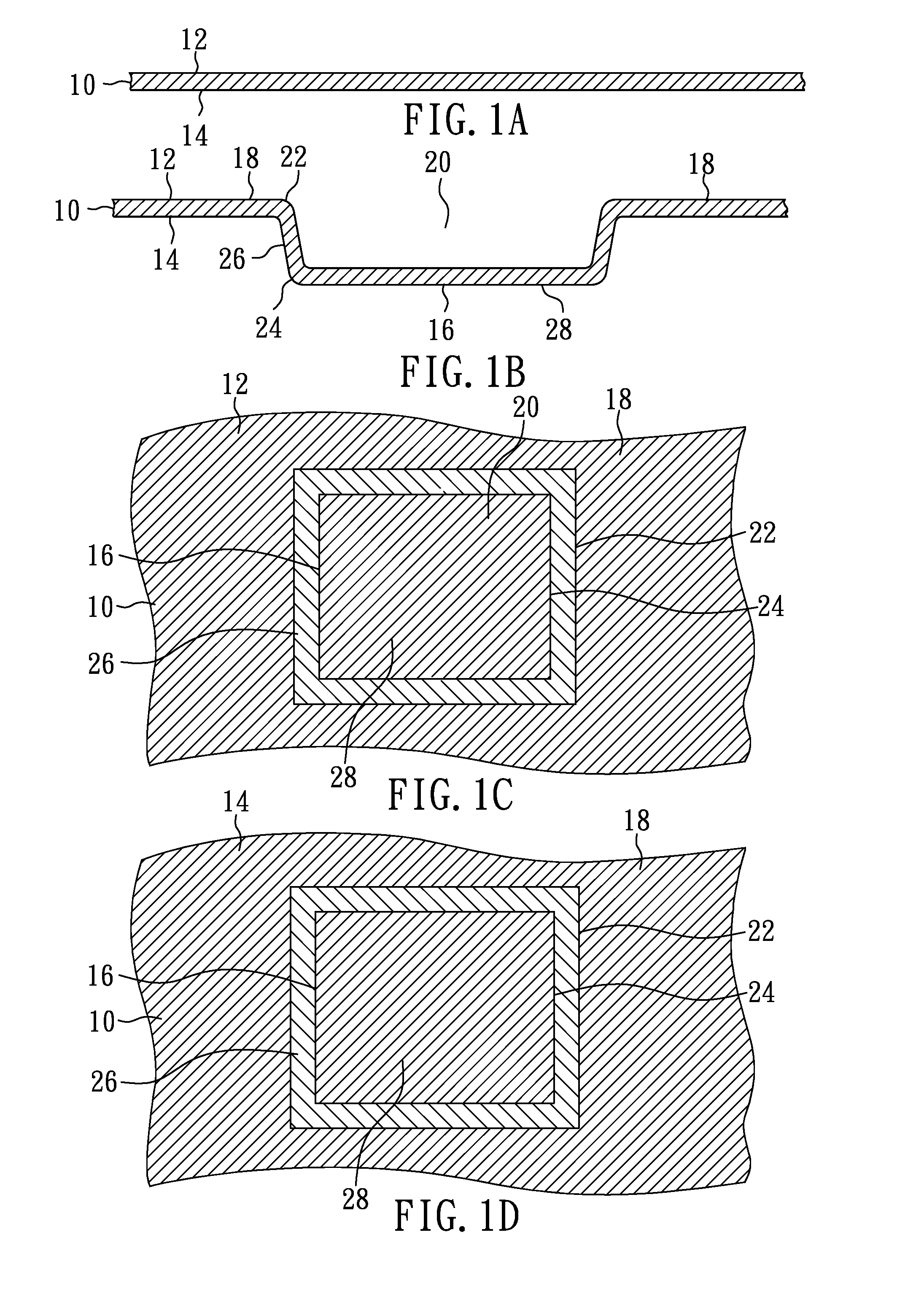
[0062]FIGS. 1A and 1B are cross-sectional views showing a method of making a sacrificial carrier with a bump and a flange in accordance with an embodiment of the present invention, and FIGS. 1C and 1D are top and bottom views, respectively, corresponding to FIG. 1B.

[0063]FIG. 1A is a cross-sectional view of sacrificial carrier 10 which is a metal plate and includes opposing major surfaces 12 and 14. Sacrificial carrier 10 is illustrated as a copper plate with a thickness of 200 microns. Copper has good flexibility and low cost. Sacrificial carrier 10 can be various metals such as copper, aluminum, alloy 42, iron, nickel, silver, gold, tin, combinations thereof, and alloys thereof.

[0064]FIGS. 1B, 1C and 1D are cross-sectional, top and bottom views, respectively, of sacrificial carrier 10 with bump 16, flange 18 and cavity 20. Bump 16 and stamped cavity 20 are formed by mechanically stamping of sacrificial carrier 10. Thus, bump 16 is a stamped portion of sacrificial carrier 10 and fl...

embodiment 2

[0119]FIGS. 6A-6I are cross-sectional views showing a method of making another cavity substrate with conductive vias in via openings of dielectric layer according to another aspect of the present invention.

[0120]For purposes of brevity, any description in Embodiment 1 is incorporated herein insofar as the same is applicable, and the same description need not be repeated.

[0121]FIG. 6A is a cross-sectional view of sacrificial carrier 10 with bump 16 extending from flange 18 in the upward direction. Sacrificial carrier 10 used in this embodiment is the same as that illustrated in Embodiment 1, except that no stamped cavity is defined in bump 16 and bump 16 has a rectangular cylinder shape with a constant diameter according to this embodiment.

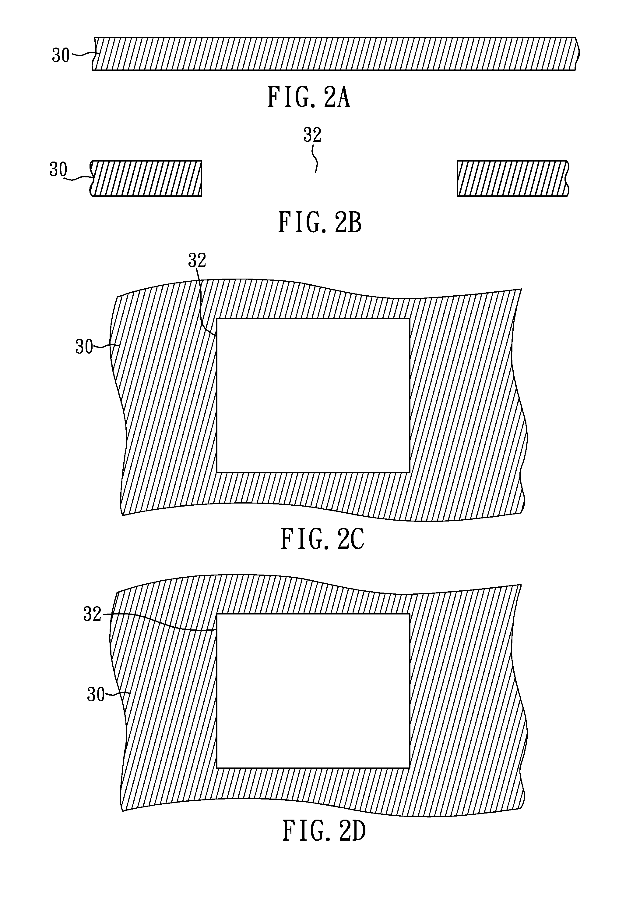
[0122]FIG. 6B is a cross-sectional view of the structure with adhesive 30 on flange 18, stiffener 33 on adhesive 30, dielectric layer 211 on stiffener 33 and interconnect substrate 201 on dielectric layer 211. Bump 16 is inserted into opening 32 an...

embodiment 3

[0137]FIGS. 7A-7F are cross-sectional views showing a method of making a three-dimensional semiconductor assembly with a cavity substrate, an embedded semiconductor device and dual build-up circuitries according to yet another aspect of the present invention.

[0138]For purposes of brevity, any description in Embodiments 1 and 2 is incorporated herein insofar as the same is applicable, and the same description need not be repeated.

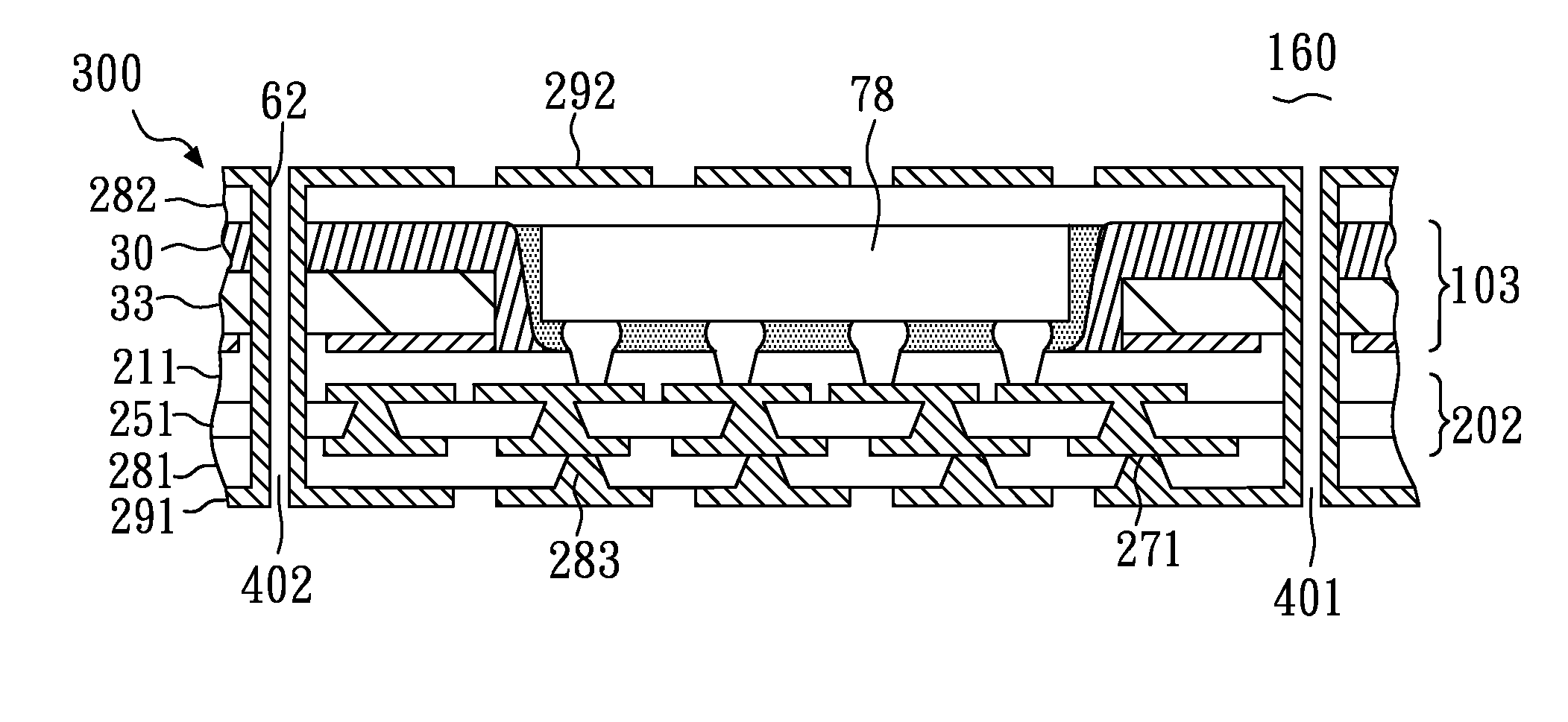
[0139]FIG. 7A is a cross-sectional view of the structure manufactured by the steps shown in FIGS. 1A-5A. In this illustration, interconnect substrate 202 includes first circuitry layer 231, first insulating layer 251, first conductive vias 263 and second circuitry layer 271.

[0140]FIG. 7B is a cross-sectional view of cavity substrate 300 with selected portions of first circuitry layer 231 exposed from cavity 31. Bump 16 and flange 18 are removed to expose dielectric layer 211, and then via openings 213 are formed through dielectric layer 211 to expose selecte...


PUM

PropertyMeasurementUnit
thicknessaaaaaaaaaa
heightaaaaaaaaaa
heightaaaaaaaaaa

Abstract

The present invention relates to a method of making a cavity substrate. In accordance with a preferred embodiment, the method includes: preparing a supporting board including a stiffener, a bump / flange sacrificial carrier and an adhesive, wherein the adhesive bonds the stiffener to the sacrificial carrier; then attaching an interconnect substrate to the supporting board using a dielectric layer; then removing the bump and a portion of the flange to form a cavity and expose the dielectric layer; and then forming a via opening in the dielectric layer to expose a selected portion of the interconnect substrate. A semiconductor device can be mounted on the cavity substrate and electrically connected to the exposed portion of the interconnect substrate. The interconnect substrate provides signal routing for the semiconductor device while the stiffener can provide adequate mechanical support for the interconnect substrate and the semiconductor device.

Description

CROSS REFERENCE TO RELATED APPLICATION[0001]This application is a continuation-in-part of U.S. application Ser. No. 13 / 197,163 filed Aug. 3, 2011, a continuation-in-part of U.S. application Ser. No. 13 / 267,946 filed Oct. 7, 2011, a continuation-in-part of U.S. application Ser. No. 13 / 299,472 filed Nov. 18, 2011, a continuation-in-part of U.S. application Ser. No. 13 / 299,495 filed Nov. 18, 2011, a continuation-in-part of U.S. application Ser. No. 13 / 532,941 filed Jun. 26, 2012 and a continuation-in-part of U.S. application Ser. No. 13 / 738,220 filed Jan. 10, 2013, each of which is incorporated by reference. This application also claims the benefit of filing date of U.S. Provisional Application Ser. No. 61 / 635,902 filed Apr. 20, 2012.[0002]U.S. application Ser. No. 13 / 197,163 filed Aug. 3, 2011, U.S. application Ser. No. 13 / 267,946 filed Oct. 7, 2011, U.S. application Ser. No. 13 / 299,472 filed Nov. 18, 2011 and U.S. application Ser. No. 13 / 299,495 filed Nov. 18, 2011 all claim the bene...

Claims


Application Information

Patent Timeline
Patent Type & Authority Applications(United States)
IPC IPC(8): H05K3/00
CPCH05K3/0094H01L23/16H01L23/5389H01L24/13H01L24/16H01L24/32H01L24/73H01L24/92H01L25/0655H01L25/0657H01L25/105H05K1/183H05K1/186H05K3/4697H01L2224/131H01L2224/16225H01L2224/16235H01L2224/16237H01L2224/32225H01L2224/73204H01L2224/97H01L2225/06517H01L2225/1023H01L2225/1058H01L2924/15153H01L2924/15311H01L2924/1533H01L2924/18161H05K2201/10674H01L2225/06572H01L23/13H01L23/49827H01L21/4857H01L23/3164H01L21/563H01L2924/15156H01L2924/12042H01L2924/3511Y10T29/49128H01L2924/014H01L2924/00H01L2224/92125
Inventor LIN, CHARLES W.C.WANG, CHIA-CHUNG
Owner BRIDGE SEMICON
Why Eureka
Try Eureka