

Semiconductor film and semiconductor device
- Summary
- Abstract
- Description
- Claims
- Application Information
AI Technical Summary
Benefits of technology
Problems solved by technology
Method used
Image

Examples
embodiment 1
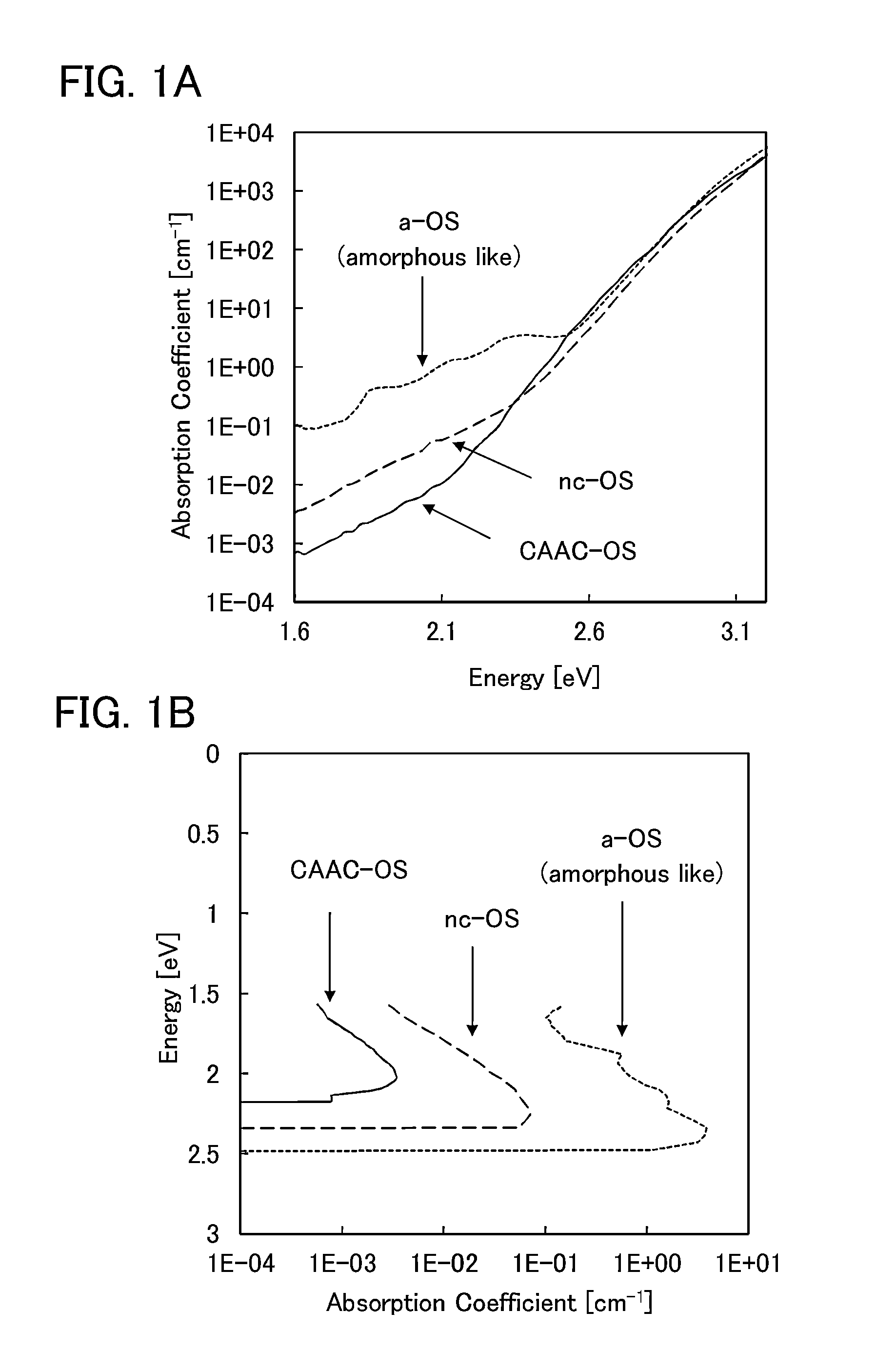
[0059]In this embodiment, an oxide semiconductor film of one embodiment of the present invention will be described.
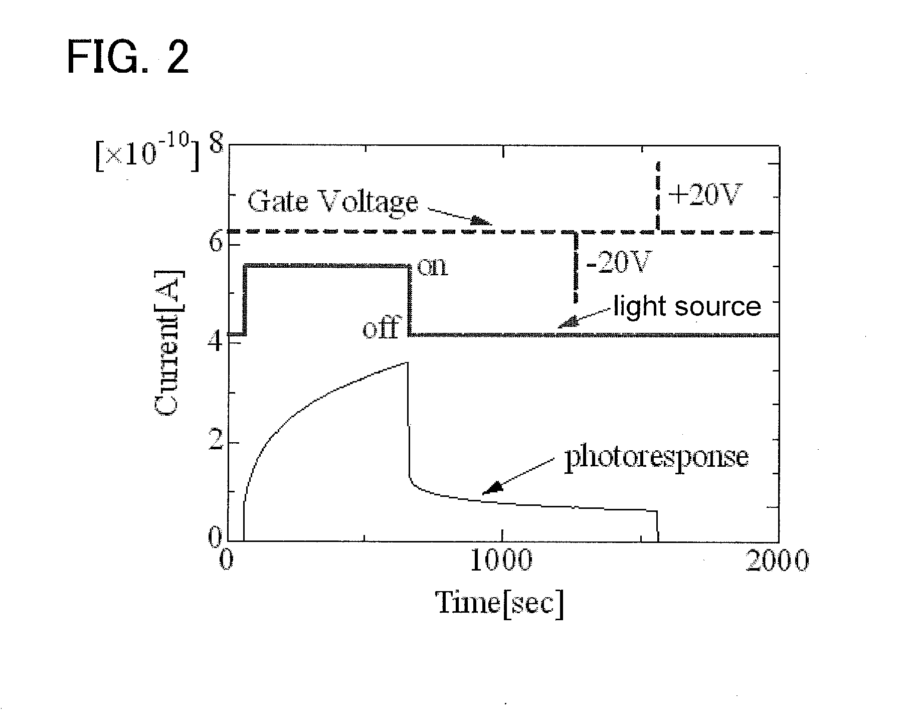
[0060]Recently, an oxide semiconductor typified by an In—Ga—Zn-based oxide (abbreviated to In—Ga—Zn—O) has attracted attention and practical application to a display device such as a liquid crystal display has begun. Electrical characteristics of a transistor including an In—Ga—Zn—O are excellent compared to those of a transistor including amorphous silicon; for example, mobility is high or an off-state current is low. However, the electrical characteristics are known to deteriorate because of light irradiation, bias-temperature (BT) stress, or the like.
[0061]Particularly in a negative bias-temperature photostress test in which a negative bias is applied to a gate of the transistor and a thermal stress is applied to the transistor while a channel formation region thereof is irradiated with light, the threshold voltage is largely shifted in the negative direction. This i...
embodiment 2
[0119]In this embodiment, a semiconductor device to which the CAAC-OS film described in Embodiment 1 can be applied will be described with reference to drawings.
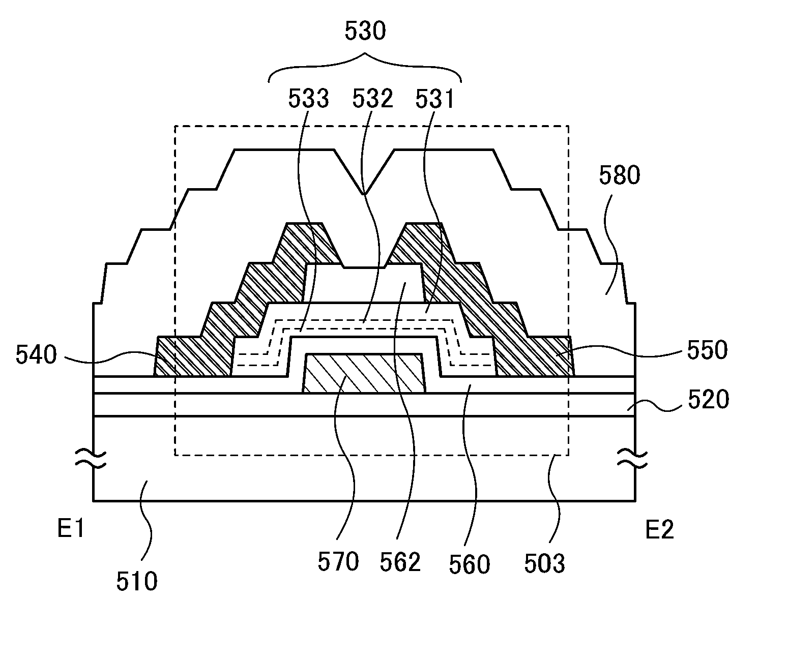
[0120]FIGS. 13A and 13B are a top view and a cross-sectional view which illustrate a transistor of one embodiment of the present invention. FIG. 13A is the top view, and a cross section taken along dashed-dotted line A1-A2 in FIG. 13A is illustrated in FIG. 13B. Note that for simplification of the drawing, some components in the top view in FIG. 13A are not illustrated. In some cases, the direction of the dashed-dotted line A1-A2 is referred to as a channel length direction.
[0121]A transistor 500 in FIGS. 13A and 13B includes a base insulating film 520 formed over a substrate 510; an oxide semiconductor layer 530 formed over the base insulating film 520; a source electrode 540 and a drain electrode 550 formed over the oxide semiconductor layer 530; a gate insulating film 560 formed over the source electrode 540 and the drain...
embodiment 3
[0183]In this embodiment, a method for manufacturing the transistor 500 described in Embodiment 2 with reference to FIGS. 13A and 13B will be described with reference to FIGS. 19A to 19C and FIGS. 20A to 20C. Note that each of the transistor 501 in FIGS. 15A and 15B, the transistor 502 in FIGS. 16A and 16B, and the transistor 503 in FIGS. 17A and 17B can be formed by, for example, changing a resist mask in a photolithography process or changing the order of steps with reference to Embodiment 2 where the transistors are described and the method for manufacturing the transistor described in this embodiment.
[0184]For the substrate 510, a glass substrate, a ceramic substrate, a quartz substrate, a sapphire substrate, or the like can be used. Alternatively, a single crystal semiconductor substrate or a polycrystalline semiconductor substrate made of silicon, silicon carbide, or the like, a compound semiconductor substrate made of silicon germanium or the like, a silicon-on-insulator (SOI...
PUM
 Abstract
Description
Claims
Application Information