

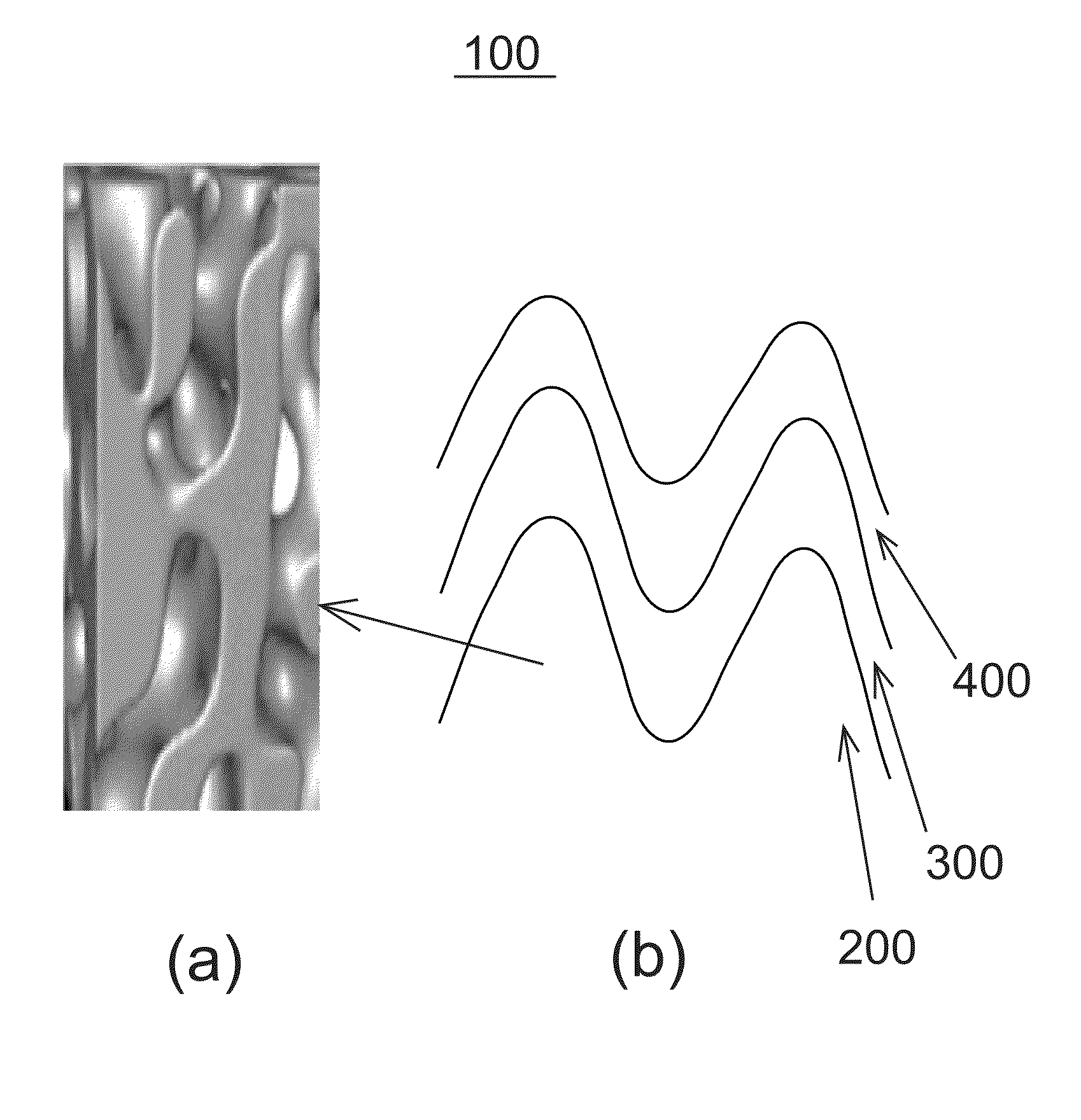
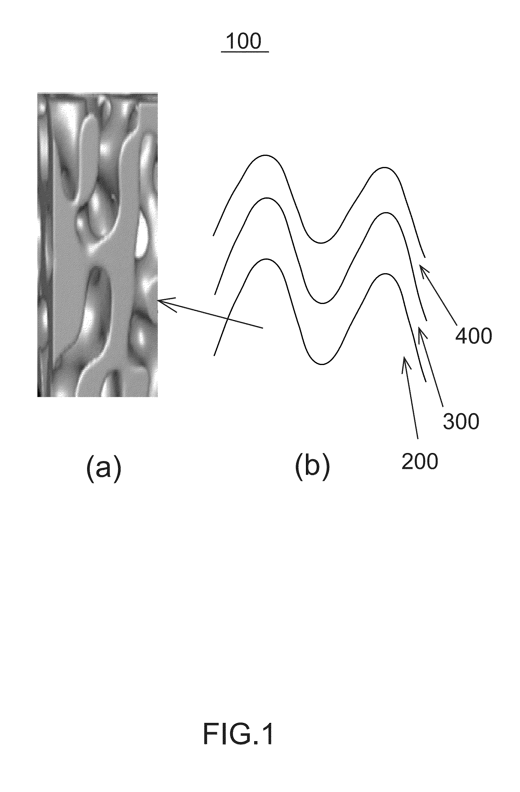
Super Capacitor And Method For Manufacturing The Same
a super capacitor and capacitor technology, applied in the direction of fixed capacitors, fixed capacitor details, transportation and packaging, etc., can solve the problems of reduced specific surface area, limited solid-state capacitor technology, and difficulty in mass production, so as to achieve simple solution process and dramatic increase of capacitance
- Summary
- Abstract
- Description
- Claims
- Application Information
AI Technical Summary
Benefits of technology
Problems solved by technology
Method used
Image

Examples
example 1
Preparation of a Capacitor
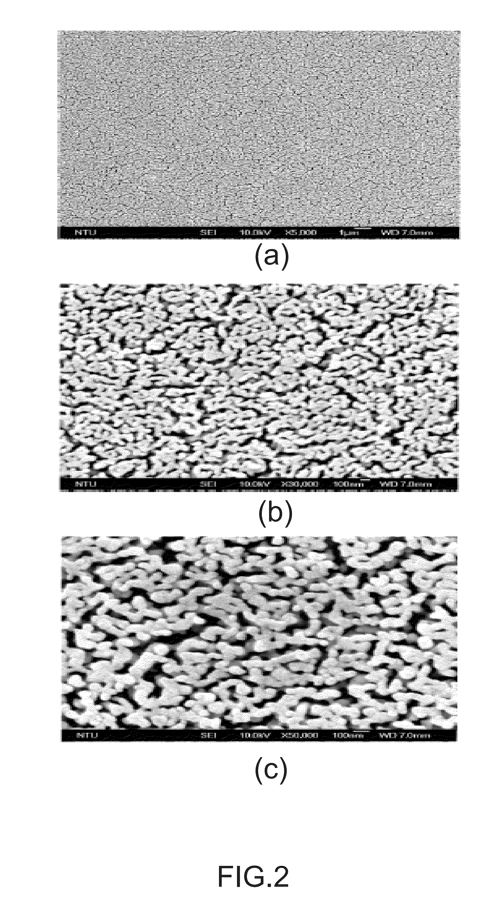
[0045]A gold-plated substrate is used and the substrate is co-evaporated with Al / Ag with an atomic ratio of 80:20 to form Al / Ag alloy thereon. 1% HCl is used to process the Al / Ag alloy at 50° C. for 10 minutes to obtain a sponge-like silver substrate as a bottom electrode. By ALD deposition, an aluminum oxide dielectric layer is deposited on the bottom electrode and its thickness is about 7 nm. Next, on the aluminum oxide dielectric layer, by ALD deposition, aluminum doped zinc oxide as a top electrode is deposited at about 150° C. and its thickness is about 20 nm so as to obtain the capacitor 1 according to the present invention.
[0046]The capacitor 1 according to the present invention is compared with a capacitor 2 made by using an AAO substrate and a capacitor 3 made by using regularly aligned carbon nanotubes. The capacitance of the capacitor 1 per unit volume is 1.225 Fcm−3 while that of the capacitor 2 is 0.1 Fcm−3 and that of the capacitor 3 is 0.023 ...
PUM
| Property | Measurement | Unit |
|---|---|---|
| thickness | aaaaa | aaaaa |
| thickness | aaaaa | aaaaa |
| diameter | aaaaa | aaaaa |
Abstract
Description
Claims
Application Information