Polycrystalline silicon rod and method for producing polysilicon

a polysilicon and polysilicon technology, applied in the field of polycrystalline silicon preparation, can solve the problems of high production cost of compact rods, increased production costs of compact rods, so as to achieve low production cost and achieve the effect of avoiding loss of yield and productivity

Inactive Publication Date: 2014-10-23
WACKER CHEM GMBH
View PDF1 Cites 3 Cited by
  • Summary
  • Abstract
  • Description
  • Claims
  • Application Information

AI Technical Summary

Benefits of technology

[0049]The specific advantage of the invention is that the last layer having exceptional properties can also be applied to silicon rods having porous and fissured morphology, which have much lower production costs compared to the compact and smooth material. As a result, it is possible to use these rods, or silicon chunks which form in the breaking of inventive rods, in the subsequent crystallization without losses in yield and productivity.
[0050]This process according to the invention gives rise to polycrystalline silicon rods that are unknown as yet in the prior art. Their features include—as described above—an outer polycrystalline layer of thickness between 0.01 and 20 mm, preferably between 0.1 and 10 mm, most preferably between 0.1 and 5 mm, and a coarser microstructure compared to the inner deposited layers.
[0051]The polycrystalline silicon is preferably deposited onto filament rods of silicon heated by direct passage of current. A filament rod is formed from two vertical rods and one horizontal rod, the horizontal rod forming a connecting bridge between the vertical rods (=u-shaped support body).
[0052]The silicon-containing component used in the reaction gas is preferably TCS or a mixture of TCS and DCS or a mixture of TCS and STC.
[0053]Preferably, during the first step of the deposition, the passage of current through the filament rod is regulated such that the rod temperature is between 1000 and 1100° C. (at the same time, the temperature measured on the underside of the bridge is between 1300 and 1413° C.). The temperature of the reaction gases in the reactor is measured and adjusted such that it is at most 650° C., and the flow rate of the chlorosilane mixture is set to its maximum value within less than 30 hours, preferably within less than 5 hours, from commencement of the supply of the chlorosilane mixture.
[0054]FIG. 1 shows the microstructure of the outer region of the inventive polycrystalline silicon rod. In the right-hand part of FIG. 1, a distinctly coarser microstructure of the outer layer is visible compared to the rod interior (left). The thickness of the outer layer is about 0.8 mm. The outer layer is formed by microcrystallites having a mean size of 30 μm or more, preferably 50 μm or more. The roughness of the surface Ra (measured to DIN EN ISO 4288, but over the shorter traversing length of 1.5 mm) is 5 mm or more.

Problems solved by technology

Between the time of reactor opening and until introduction into storage or further processing, the material deposited, however, is exposed to environmental influences, particularly dust particles.
The compact rods are more costly to produce, but often lead to better yields in subsequent crystallization steps.
Each of these parameters, however, is subject to natural limits, exceedance of which disrupts the production process (according to the configuration of the reactor used, the limits are somewhat different).
The effect of an excessively high rod temperature may be that the morphology of the silicon rods to be deposited does not become compact enough to provide a sufficient cross-sectional area for the current flow which rises with the growing rod diameter.
If the current density becomes too high, this can cause silicon to melt.
In the mechanical manufacture of cut rods, FZ rods and recharging rods by means of sawing, the surface thereof is contaminated significantly.
Typically, a porous and fissured morphology has an adverse effect on the crystallization characteristics.
This particularly affects the demanding CZ process, in which porous and fissured chunks were not usable because of the economically unacceptable yields.
The cleaning, which is normally effected by wet-chemical means with one or more acids or acid mixtures (see, for example, U.S. Pat. No. 6,309,467 B1), is very inconvenient and costly, but generally improves the product properties.
In the case of silicon chunks having porous or fissured morphology, the wet-chemical cleaning, however, cannot bring about any improvement in performance.

Method used


Image

  • Polycrystalline silicon rod and method for producing polysilicon
  • Polycrystalline silicon rod and method for producing polysilicon

Examples


example 5

[0075]In this example, the procedure was as in Example 2, with the difference that, after the deposition, polysilicon rods were covered with polyethylene sacks and deinstalled from the deposition reactor under a nitrogen atmosphere. This alteration surprisingly increased the yield in the single-crystal pulling operation by 2.1% to 92.9%.

example 6

[0076]In this example, compact polysilicon rods were deposited. The deposition proceeded up to the diameter of 149 mm as described in US 2010 / 219380 A1 Comparative example 1. Then the process parameters were altered as follows: the rod temperature was raised by 120° C. to 1150° C., the TCS feed was lowered to 0.05 kmol / h per 1 m2 of rod surface area and the TCS concentration to 4 mol %. These process parameters were maintained until the rods had attained the diameter of 150 mm.

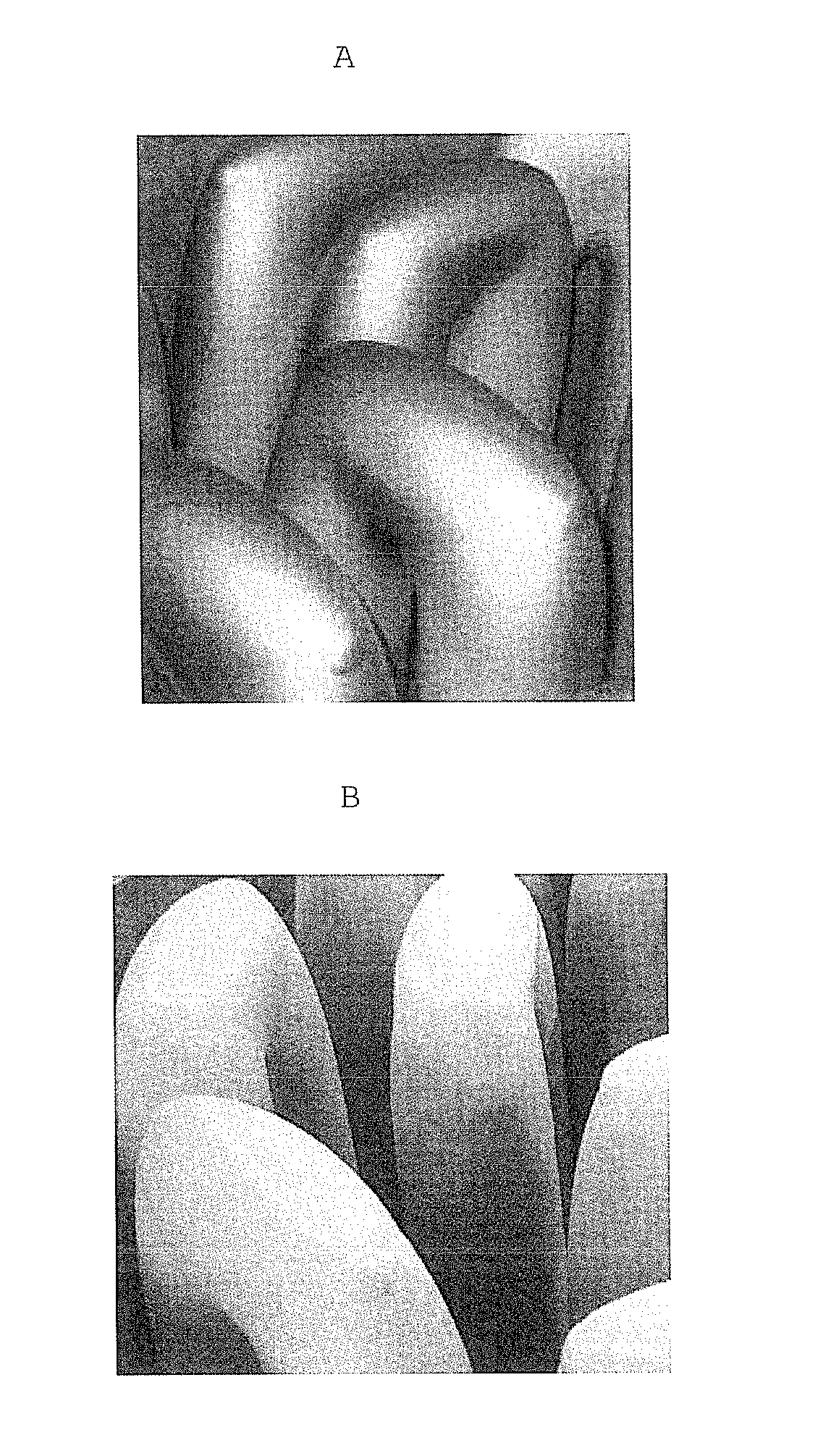
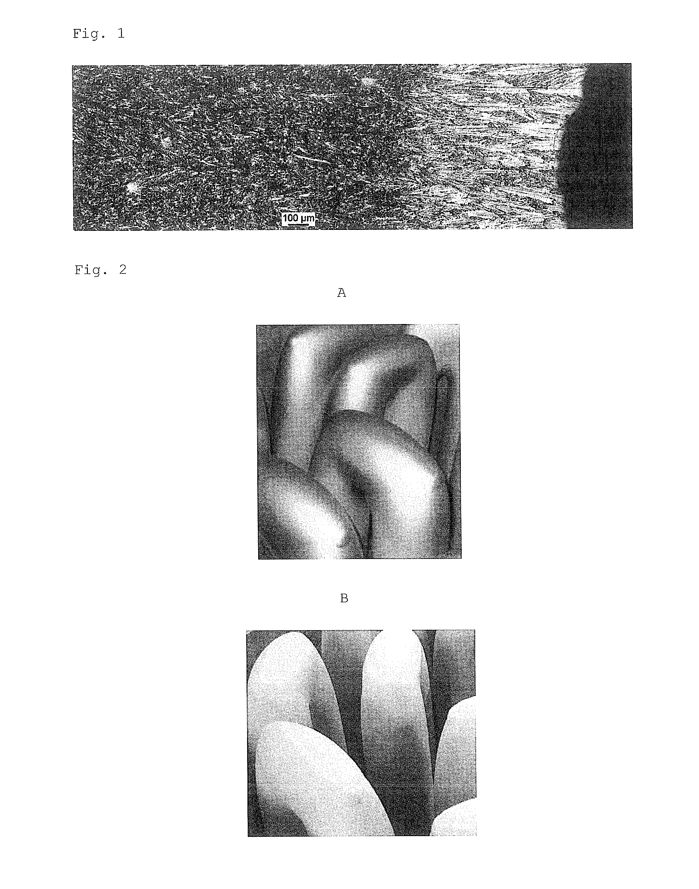
[0077]The inventive rods obtained were shiny and had an outer layer of thickness 0.5 mm with a distinctly coarser microstructure. The mean crystallite size in the rod interior was 11 μm, and in the outer layer was 37 μm. The roughness of the rod surface had an Ra value of 5.1 μm.

[0078]Subsequently, the rods were broken into silicon chunks by a low-contamination method and dedusted. With this inventive material, it was possible to achieve a yield of 95.2% in the pulling operation.

example 7

[0079]In this example, porous and fissured polycrystalline silicon rods were deposited. The deposition proceeded as far as 148 mm essentially as described in US 2010 / 219380 A1, Example 1. The rod temperature was 1075° C. At the same time, the temperature measured on the underside of the bridge as described therein was 1300 to 1413° C.

[0080]Then, the process parameters were altered as follows: the rod temperature was raised by 125° C. to 1200° C., the feed of the TCS / DCS mixture was lowered to 0.03 kmol / h per 1 m2 of rod surface area and the TCS / DCS concentration to 3 mol %. These process parameters were maintained until the rods had attained the diameter of 150 mm.

[0081]The inventive rods obtained were shiny gray and had an outer layer of thickness 1.0 mm having a distinctly coarser microstructure. The mean crystallite size in the rod interior was 16 μm, and in the outer layer was 52 μm.

[0082]The roughness of the rod surface had an Ra value of 5.6 μm.

[0083]Subsequently, the rods wer...


PUM

PropertyMeasurementUnit
thicknessaaaaaaaaaa
thicknessaaaaaaaaaa
surface roughnessaaaaaaaaaa

Abstract

Polycrystalline silicon rods produced by the Siemens process produce a higher yield of CZ crystals when the process parameters are modified in a second stage of deposition such that an outer layer of larger crystallites having a mean swize>20 μm is produced. Harvesting of these polycrystalline rods and conventional rods by enclosing them in a plastic bag or sheath prior to removal from the reactor also surprisingly increase the yield of CZ crystals grown from a melt containing the sheathed rods.

Description

CROSS-REFERENCE TO RELATED APPLICATIONS[0001]This application is the U.S. National Phase of PCT Appln. No. PCT / EP2012 / 075208 filed Dec. 12, 2012, which claims priority to German Application No. 10 2011 089 449.7 filed Dec. 21, 2011, the disclosures of which are incorporated in their entirety by reference herein.BACKGROUND OF THE INVENTION[0002]1. Field of the Invention[0003]The present invention relates to the preparation of polycrystalline silicon by chemical vapor deposition, e.g. by the Siemens process.[0004]2. Description of the Related Art[0005]Polycrystalline silicon (polysilicon for short) serves as a starting material for production of monocrystalline silicon for semiconductors by the Czochralski (CZ) or zone melting (FZ) process, and for production of mono- or polycrystalline silicon by various pulling and casting processes for production of solar cells for photovoltaics.[0006]Polycrystalline silicon is generally produced by means of the Siemens process. In this process, in...

Claims


Application Information

Patent Timeline
Patent Type & Authority Applications(United States)
IPC IPC(8): C01B33/029
CPCC01B33/029C01B33/035Y10T428/298Y10T428/2978
Inventor SOFIN, MIKHAILDORNBERGER, ERICHPECH, REINER
Owner WACKER CHEM GMBH
Why Eureka
Try Eureka