Display device and electronic device including the display device

a technology of electronic devices and display devices, applied in semiconductor devices, instruments, electrical devices, etc., can solve the problems of increasing manufacturing costs, and achieve the effects of reducing the manufacturing steps of display devices, low cost, and favorable characteristics

Active Publication Date: 2014-11-13
SEMICON ENERGY LAB CO LTD
View PDF8 Cites 27 Cited by
  • Summary
  • Abstract
  • Description
  • Claims
  • Application Information

AI Technical Summary

Benefits of technology

[0010]In the display device disclosed in Patent Document 3, a pixel electrode serving as one electrode of a capacitor needs to be formed in a step different from a step of forming an oxide semiconductor layer included in a transistor, which increases the manufacturing cost.
[0012]In view of the above problems, an object of one embodiment of the present invention is to provide a novel display device including a transistor that includes an oxide semiconductor and thus has favorable characteristics, a pixel electrode electrically connected to the transistor, and a capacitor electrically connected to the pixel electrode. Another object of one embodiment of the present invention is to provide a display device that can be manufactured at low cost.
[0015]Note that the second oxide semiconductor layer serving as the pixel electrode and the one electrode of the capacitor can also be referred to as an oxide semiconductor layer having high conductivity. The oxide semiconductor layer having high conductivity can be formed as follows. When hydrogen is added to an oxide semiconductor including oxygen vacancies, hydrogen enters oxygen vacant sites and forms a donor level in the vicinity of the conduction band. As a result, the conductivity of the oxide semiconductor layer is increased, so that the oxide semiconductor layer becomes conductive. Such an oxide semiconductor layer having become conductive can be referred to as an oxide conductor layer. An oxide semiconductor layer generally has a visible light transmitting property because of its large energy gap. An oxide conductor layer is an oxide semiconductor having a donor level in the vicinity of the conduction band. Therefore, the influence of absorption due to the donor level is small, and an oxide conductor layer has a visible light transmitting property comparable to that of an oxide semiconductor layer.
[0016]According to one embodiment of the present invention, the first oxide semiconductor layer serving as the channel formation region of the transistor and the second oxide semiconductor layer serving as the pixel electrode can be formed at the same time. Furthermore, the second oxide semiconductor layer also serves as the one electrode of the capacitor; thus, a step of further forming a conductive layer is unnecessary, reducing the manufacturing steps of the display device. This enables the display device to be manufactured at low cost.
[0019]According to one embodiment of the present invention, the one electrode of the capacitor is formed at the same time as the gate electrode of the transistor. The other electrode of the capacitor is formed at the same time as the oxide semiconductor layer of the transistor. Note that the other electrode of the capacitor also serves as the pixel electrode. In addition, the dielectric layer of the capacitor is formed at the same time as the gate insulating layer of the transistor. Thus, a step of further forming a conductive layer and / or a dielectric layer to form a capacitor and / or a pixel electrode is unnecessary, reducing the manufacturing steps of the display device. This enables the display device to be manufactured at low cost.
[0020]According to one embodiment of the present invention, it is possible to provide a novel display device including a transistor that includes an oxide semiconductor and thus has favorable characteristics and, a pixel electrode electrically connected to the transistor, and a capacitor electrically connected to the pixel electrode. Furthermore, the display device can be manufactured at low cost.

Problems solved by technology

In the display device disclosed in Patent Document 3, a pixel electrode serving as one electrode of a capacitor needs to be formed in a step different from a step of forming an oxide semiconductor layer included in a transistor, which increases the manufacturing cost.

Method used


Image

  • Display device and electronic device including the display device
  • Display device and electronic device including the display device
  • Display device and electronic device including the display device

Examples


embodiment 1

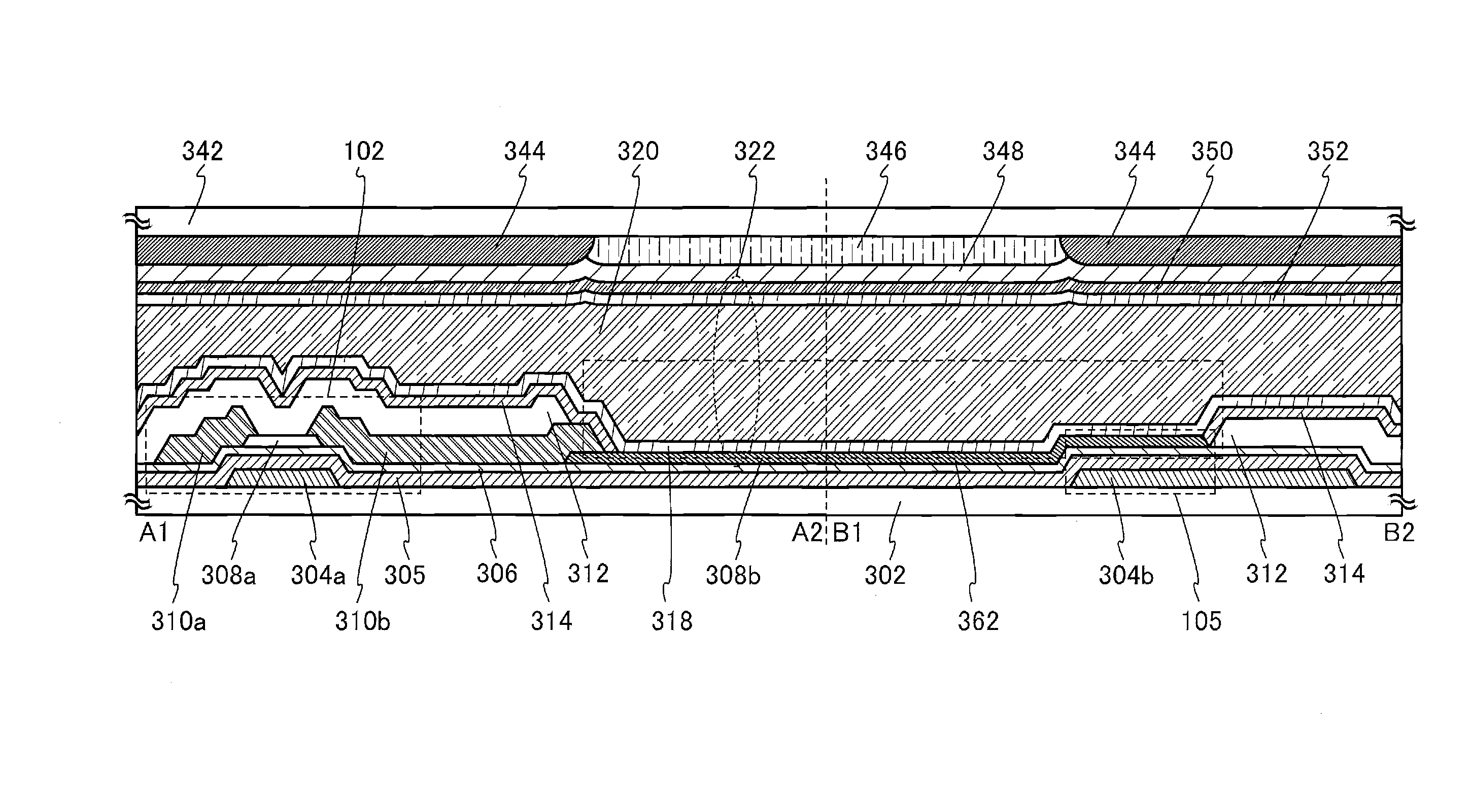
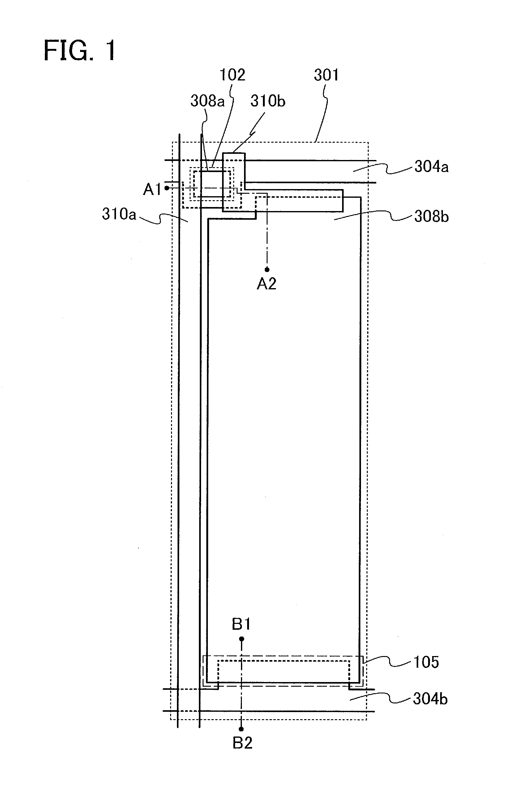
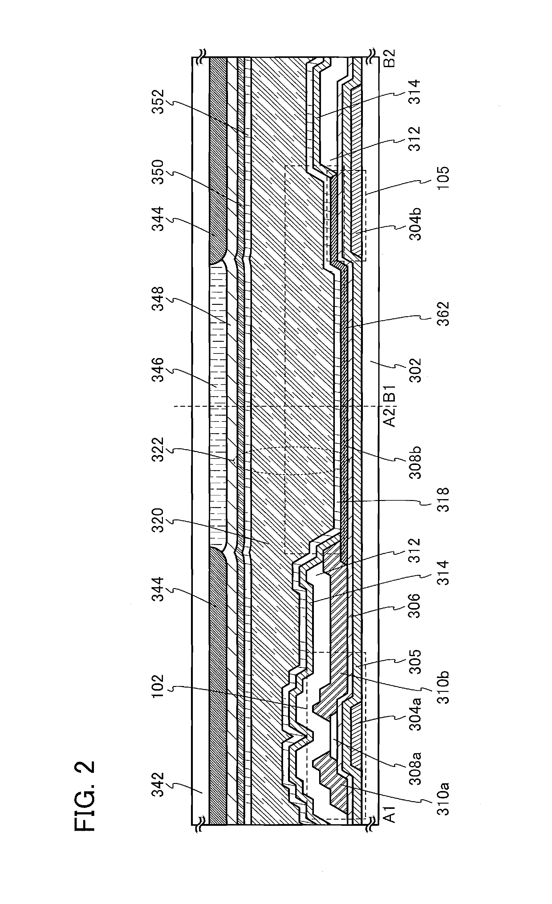
[0036]In this embodiment, a display device of one embodiment and a manufacturing method of the display device of one embodiment of the present invention will be described with reference to FIG. 1, FIG. 2, FIGS. 3A to 3C, FIGS. 4A to 4C, FIG. 5, FIGS. 6A to 6C, FIGS. 7A and 7B, and FIG. 8.

[0037]FIGS. 1 and 2 illustrate a structural example of the display device. FIG. 1 is a plan view of a pixel 301 included in a display device, and FIG. 2 is a cross-sectional view along dashed-dotted lines A1-A2 and B1-B2 in FIG. 1. Note that in FIG. 1, some components (e.g., insulating layers 305 and 306) of the pixel 301, a display element provided over the pixel 301, and the like are not illustrated for simplicity.

[0038]In the pixel 301 in FIG. 1, a conductive layer 304a serving as a scan line extends substantially perpendicularly to a signal line (in the horizontal direction in the drawing). The conductive layer 310a serving as the signal line extends substantially perpendicularly to the scan lin...

embodiment 2

[0171]In this embodiment, an example of an oxide semiconductor layer that can be used for the transistor, the electrode of the capacitor, and the pixel electrode described in Embodiment 1 will be described.

[0172]A structure of an oxide semiconductor layer will be described below.

[0173]An oxide semiconductor layer is classified roughly into a single-crystal oxide semiconductor layer and a non-single-crystal oxide semiconductor layer. The non-single-crystal oxide semiconductor layer includes any of an amorphous oxide semiconductor layer, a microcrystalline oxide semiconductor layer, a polycrystalline oxide semiconductor layer, a c-axis aligned crystalline oxide semiconductor (CAAC-OS) film, and the like.

[0174]First, a CAAC-OS film will be described.

[0175]The CAAC-OS film is one of oxide semiconductor films including a plurality of crystal parts, and most of the crystal parts each fit inside a cube whose one side is less than 100 nm. Thus, there is a case where a crystal part included ...

embodiment 3

[0215]In this embodiment, a display device of one embodiment of the present invention will be described with reference to drawings. Note that portions similar to those in the above embodiments and portions having functions similar to those in the above embodiments are given the same reference numerals, and detailed descriptions thereof are omitted.

[0216]FIG. 9A illustrates an example of a display device. The display device in FIG. 9A includes a pixel portion 200, a scan line driver circuit 204, a signal line driver circuit 206, m scan lines 207 that are arranged in parallel or substantially in parallel and whose potentials are controlled by the scan line driver circuit 204, and n signal lines 209 that are arranged in parallel or substantially in parallel and whose potentials are controlled by the signal line driver circuit 206. The pixel portion 200 includes a plurality of pixels 301 arranged in a matrix. Capacitor lines 215 that are arranged in parallel or substantially in parallel...


PUM

PropertyMeasurementUnit
drain voltageaaaaaaaaaa
off-state currentaaaaaaaaaa
channel lengthaaaaaaaaaa

Abstract

To provide a display device including a transistor that includes an oxide semiconductor and has favorable characteristics, a pixel electrode electrically connected to the transistor, and a capacitor electrically connected to the pixel electrode. To provide a display device that can be manufactured at low cost. The display device includes a display element including a pixel electrode, a transistor that performs switching of the display element and includes a first oxide semiconductor layer serving as a channel formation region, a capacitor that is electrically connected to the display element and includes a dielectric layer between a pair of electrodes. The pixel electrode is a second oxide semiconductor layer formed on the same surface as that on which the first oxide semiconductor layer is formed, and also serves as one electrode of the capacitor.

Description

BACKGROUND OF THE INVENTION[0001]1. Field of the Invention[0002]The present invention relates to a display device and an electronic device using the display device.[0003]2. Description of the Related Art[0004]Transistors used for most flat panel displays typified by a liquid crystal display device and a light-emitting display device are formed using silicon semiconductors such as amorphous silicon, single crystal silicon, and polycrystalline silicon provided over glass substrates. Further, transistors using such silicon semiconductors are used in integrated circuits (ICs) and the like.[0005]In recent years, attention has been drawn to a technique in which, instead of a silicon semiconductor, a metal oxide exhibiting semiconductor characteristics is used in transistors. Note that in this specification, a metal oxide exhibiting semiconductor characteristics is referred to as an oxide semiconductor.[0006]For example, such a technique is disclosed in which a transistor is fabricated usi...

Claims


Application Information

Patent Timeline
Patent Type & Authority Applications(United States)
IPC IPC(8): H01L27/12G02F1/1368
CPCH01L27/1255H01L27/127H01L27/1225G02F1/1368H01L27/1248G02F1/136213H10K59/123H10K59/1213H10K59/1216G02F1/133345G02F1/13439G02F2201/123G02F2202/10H01L29/7869
Inventor MIYAKE, HIROYUKIYAMAZAKI, SHUNPEI
Owner SEMICON ENERGY LAB CO LTD
Why Eureka
Try Eureka